IC LM2596 Datasheet, Schematic, dc to dc buck converter
The LM2596 is a popular voltage regulator/ buck converter IC ideally suited for convenient design of a step−down, or you can say step-up switching regulator. With excellent line and load regulation, it can drive a total 3.0 Amps of load.
These power converters are available in fixed output voltages of 3.3V, 5V, 12V, and an adjustable output. The device with an adjustable output version is internally compensated to minimize the number of external components to simplify the power supply design circuits.
In comparison with popular three-terminal linear regulators, the LM2596 buck converter is significantly more efficient due to its switch-mode power supply feature, especially when input voltage is high.
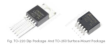
The LM2596 operates at a higher switching frequency of 150 kHz, which means smaller sized filter capacitors would be needed as compared to lower frequency switching regulators. If talking of packaging, it is available in a standard 5−lead TO−220 package with several lead bend options (check datasheet), and the D2PAK surface mount package.
Note: IC CA2596 could be an alternative to LM 2596 dc to dc buck converter IC, if later is not available. Thus, you can use an IC CA2596 dc to dc buck converter for the same purpose. It has very similar working and specifications, you can use the below-mentioned schematic for CA2596 or refer to the datasheet for details.
Also check, specifications of LM2596 HV series.
Features of LM2596 series:
The main features include a max of ±4{42041a7992ac3be9e9e29c856254fb498d8c7935d7cf8512da6802e8688e734a} tolerance at output terminals when specified input voltages and load conditions are met. External pin(5) is implemented to ON/OFF the power converter.
- Available in a fixed 3.3V, 5V, 12V and an adjustable output voltage range of 1.23 V − 37 V.
- Maximum of 3.0 A output load current guaranteed.
- Available in TO-220 and TO-263 packages.
- Wide input voltage range up to 40 Volts.
- A 150 kHz fixed frequency internal oscillator.
- It requires only 4 external components.
- TTL shutdown capability (for digital/ analog ON/OFF)
- Low power standby mode, as low as 80 uA when in standby mode.
- Internal thermal shutdown and current limit protection.
Schematic diagram of LM2596 dc to dc buck converter module:
Components required:
IC 2596 TO-220 dip package with heatsink, L1 = inductor = 33uH, R1 = 5kΩ, R2 = variable resistor 100kΩ or higher, C1 = 100uF 50V, C2 = 220uF 50V, Schottky stitching diode = IN5822 (any alternative will work).
Check below circuit diagram for adjustable dc to dc buck converter using LM 2596 ADJ schematic of the IC.
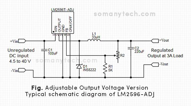
The above image is self-explanatory in terms of wiring diagram/ circuit connections. Please ensure that the input voltage must be (1.5 volts) higher than the required output voltage. Also follow ‘Circuit Design Rules’ while implementing a PCB (printed circuit board) design.
In the general, input could be between 4.5V and 40V. And the output could be derived in the range of 1.23V to 35V, and maximum up to 3 Amps.
Also check the LM2596 Resistor Calculator Tool Here!
The output of the circuit depends on the FB (feedback voltage). We just needed to add R1 and R2 to the feedback pin(4) as shown in the schematic. The feedback voltage is dependent on the value of resistor R1 and R2. Thus, to make the output voltage controllable add a variable resistor and get the desired voltage according to the following formula:
Vout = Vref(1+R2/R1)
Where, Vref= 1.23 Volts
And, R1 could be between 1KΩ to 5KΩ, choose R2 be a variable resistor.
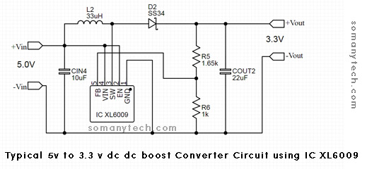
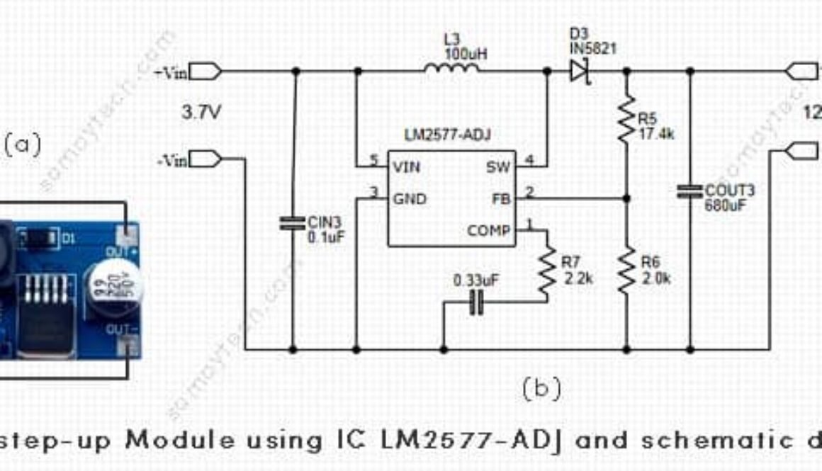
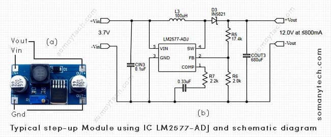
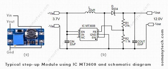
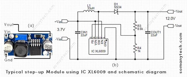
Also check, 3.7v to 5v Boost Converter Circuit
The capacitor C1/C3 are input filter capacitor that stabilize change in DC input going to the IC. Also, capacitor C2/C4 are output filter capacitors.
- If you are working on full range input and output voltages. Then you must choose output capacitor accordingly (voltage ratings must be higher than that of operating voltage range).
- Also choose capacitor value as shown on this post or that of recommended in datasheets of respective IC.
Check below circuit diagram for dc to dc buck converter using fixed version of the IC.
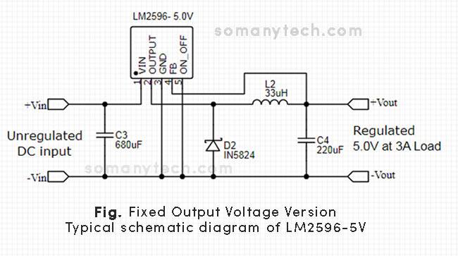
This is a 5v fixed version of the IC, you can use 3.3V and 12V version of IC as well in the above circuit. (schematic would be same for all fixed version of LM2596 IC)
LM2596 Datasheet :
For more detailed technical information on this power converter, check lm2596 IC datasheet here.
Pinout diagram of LM2596:
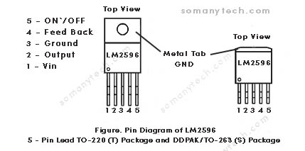
There are five total pins on the LM2596, as follows:
Pin(1)= Input voltage pin= This pin connects the input supply with the input filter capacitor to prevent voltage spikes at input.
Pin(2)= Output pin (circuit is different for fixed regulators and Adj. version)
Pin(3)= Ground pin = This pin is connected to the ground and a heat-sink.
Pin(4)= Feedback pin = This pin returns feedback voltage to the internal comparators for regulation.
Pin(5)= ON/OFF = It is a negative trigger terminal, this means grounding (0 volts) will enable and 1.3 V or higher volts will disable the operations of the internal circuit. This pin is used to standby the voltage regulator circuit to current consumption as low as 80uA.
Applications of LM2596 buck converter:
- In power supply circuits of lithium-ion battery chargers
- Any type of load that takes 3 Amperes of current.
- Simple applications where high efficiency step−down or step-up regulators are required.
- Can be used as a high efficiency pre−regulator for Linear Regulators.
- Negative Step−Up Converters.
(All the datasheets and IC’s nomenclature ownership belongs to the respective semiconductor company. The purpose of this post is to elaborate the applications of popular voltage regulators)

