The TC4056 is a linear li-ion battery charger IC that is generally used in devices to charge 18650 li-ion cells. This is a charge controller IC which is designed to be used with all 3.7v of lithium ion cells, including Li-Polymer, Li-ion, and LiFePO4 batteries. In this article we will be discussing the circuit diagram of the TC4056 Lithium Ion Battery Charger module, components on the module.
If you are looking for alternatives to TC4056A then, there are several li-ion battery charger ICs such as the TP4056, TP5100, and TP5000. These ICs have similar functions to that of the TC4056A, but they have slightly different specifications, features and application.
The TP4056, TP5100, and TP5000 are alternatives to the TC4056, and they can be used as a substitute charge controller. Before selecting an alternative IC, it is essential to carefully examine the specific requirements of the application.
TC4056 Schematic & Circuit diagram
Below is the simple circuit diagram for the 3.7 V battery charger schematic according to the datasheet of TC4056 with temperature sense disabled. The circuit diagram for the TC4056A is simple, consisting of the main IC and a few supporting components such as resistors, capacitors, and LEDs. The schematic includes the input and output connections, as well as the output current control.
In the charging phase, only the Red LED glows, and in the fully charged state, only the Green LED glows. These indicators are connected to pin number 7 and pin number 6 respectively.
So here’s the diagram: How to wire a TC4056?
Components required:
IC TC4056, 2x LED indicator, 2x Cap= 10uF, Rprog= 1.2KΩ, 2x Resistor= 1KΩ, Rs= 0.4Ω, 3.7V Lithium cell, micro usb/ usb c female connector, pcb.
Note:
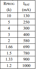
This circuit can be used only for charging purposes. Rprog is chosen to be 1.2KΩ for 1000mA of output current, this can be changed by setting different values of Rprog. If Rprog is chosen to be 2KΩ then battery will be charge at 580mA of output current.
You can manually set the charging current (IBAT) of the lithium ion cell by selecting a value for the Rprog value. In all modes during charging, the voltage on pin 2 can be calculated with respective to charging current as follows:
The Rprog(KΩ) vs Ibat(mA) can be determined using following table:
The TC4056A and its alternatives ICs have the battery protection features to ensure safe and reliable charging. Like, it has over-voltage protection, which prevents the battery from being charged to a voltage level that is too high. It also has thermal protection, which cuts off the current when the chip gets overheated due to any reason, and also has short-circuit protection.
TC4056 Module:
IC TC4056 is also available as a module, which has all the components on board required for functioning. This module makes it easy for DIY projects, as it eliminates the need for manual soldering and component placement. TC4056A modules can be purchased online or through electronic component distributors.
TC4056 Pinout:
The TC4056 has a total of eight pins, all of them are used in the schematics. The pinout of the TC4056A is as follows:
VCC+: This is the positive input terminal.
PROG-: This is the terminal for determining the charging current.
BAT+: This is the positive terminal of the battery being charged.
CHRG: This is the indicator pin of the battery being charged.
STDBY: This is the status output pin, which indicates the battery is not connected.
GND: This is the ground pin.
TEMP: This is the thermal protection pin, which provides protection against overheating.
CE: This is the charge enable pin, ie., switch for charging process.
The pinout of the TC4056A and its circuit diagram are also straightforward and well-documented, making it easy to use in a variety of battery charging applications.
An 18650 battery charger circuit is specifically used to safely charge 3.7 volt lithium ion batteries. 18650 batteries are lithium-ion cells that are commonly used in several electronic devices such as laptops, bluetooth speakers, portable consumer electronics and power banks. They are called 18650 batteries because they are cylindrical, 18mm in diameter and 65mm in length.
In this piece, we will discuss common 18650 battery charger circuits and popular charge controller modules. Also, it will be helpful for DIY lithium battery charger circuits.
There are different ways to design an 18650 battery charger circuit, all of them have common basic building blocks. This circuit consists of a charging controller, a power supply, and a charging port:
The main block from above is the charge controller. The charging controller regulates the charging process to ensure that the battery is charged safely and efficiently. The charge controller sets and monitors the battery’s voltage and charge current to determine according to specific needs of a particular lithium battery. It also prevents the battery from being overcharged and deep discharge. This helps increase the life of a lithium battery and thus the device.
The power supply could be any AC adapter, a USB port, or a solar panel. The power supply provides stable DC voltage that directly can’t be used to charge li-ion batteries, thus a charge controller is used. The charging port is usually a female DC jack or a micro USB port. The charging port is an input to the charging controller, which monitors the battery and controls the charging process.
18650 battery charger circuit using TP4056 charge controller IC:
The TP4056 is a popular and most widely used battery charging controller IC. It is a simple and cost-effective IC that is designed for low-power portable electronic devices such as power banks. One of the main advantages of the TP4056 IC is its low cost and simplicity. It has a simple circuit and does not require any additional components to function. It is also widely available and can be easily purchased from online retailers or electronics suppliers.
The TP4056 IC has a built-in charge controller and voltage regulator that is capable of charging lithium-ion or lithium-polymer batteries. It supports USB and AC/DC power sources, and has several safety features to protect the battery and the charger from being damaged.
You could implement an 18650 battery charger circuit using TP4056 in two ways, one directly with the TP4056 module available in the market and other with the TP4056 charger IC. Both are discussed and explained in detail below:
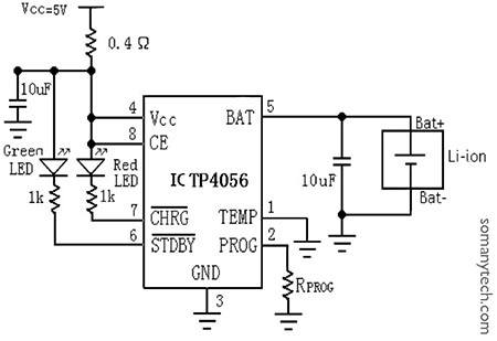
Below is the simple circuit diagram for the 18650 battery charger schematic according to the datasheet of Tp4056 with temperature sense disabled.
Only Red LED glows when the battery is charging and only Green LED glows when the battery is fully charged. These indicators are connected to pin number 7 and pin number 6 respectively.
So here’s the diagram: How to wire a TP4056?
Components required:
IC TP4056, 2x LED indicator, 2x Cap= 10uF, Rprog= 1.2KΩ, 2x Resistor= 1KΩ, Rs= 0.4Ω, 3.7V Lithium cell, micro USB/ USB c female connector, pcb.
Note:
This circuit can be used only for charging purposes. Rprog is chosen to be 1.2KΩ for 1000mA of output current, this can be changed by setting different values of Rprog. If you have two 18650 lithium batteries, then by connecting them in parallel, each battery will charge at 500mA of current. If you connect three then it will charge them at 1000/3 mA each, thus it will take longer to fully charge each battery. To charge 18650 battery with 2000mA current you need to use module with IC TP5100 check here TP5100 circuit and datasheet.
The charging current (IBAT) of the li ion cell can be set manually by choosing the value of Rprog. In all modes during charging, the voltage on pin 2 can be used to measure the charge current as follows:
The Rprog(KΩ) vs Ibat(mA) can be determined using following table :
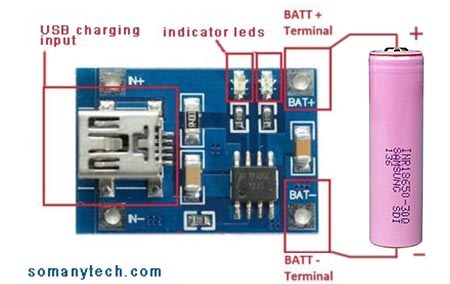
Tp4056 module: 18650 Li-ion 3.7 v battery charger circuit
Overall, the TP4056 is a good option for charging single-cell lithium-ion or lithium-polymer batteries in low-power applications. It is simple, cost-effective, and widely available, which makes it a popular choice among designers and manufacturers.
FAQ:
How many batteries can charge in TP4056?
You can charge one or more lithium battery cells with TP4056, but note that it has max 1000mA of charging current. So, when charging multiple cells you have to connect them in parallel. Also the charging current will be divided among them, which will make charging slower. It is recommended to charge one or two cells at a time with TP4056 module.
What is the maximum output current of TP4056?
The maximum output current of TP4056 is 1000mA. It can be programmed to provide charging current from 130mA to 1000mA by changing the value of Rprog.
Are you in search of the top best Arduino projects? If yes, then keep reading this post, it can be assured that you would choose one of the mentioned projects below for you.
Arduino projects have revolutionized the electronics/ electrical engineering projects and DIY sector in the present day. First-timers can find these projects quite engaging, especially if they are building their first project. You would be best off choosing Arduino projects if you have a specific interest in technology and wish to do interactive projects with it.
Now take a look at what Arduino has to offer and why you chose it?
Why only Arduino projects?
Arduino as a microcontroller being used in projects over the globe for a long time now. It also has a huge online community for supporting each other in hardware and code debugging. These community members are active learners, experts, professionals, and Arduino programmers. The Arduino hardware and Arduino software IDE is open-source and thus low cost. Below are the features that made it popular:
As compared to the other micro-controller platforms it is very cheap. Arduino boards start from less than $25 for Arduino micro from the official website, but the Chinese made boards even cost half the price of that.
The Arduino IDE is a cross platform program and supported by most of the operating systems, also has third party online editors/ simulator like: free online simulator wokwi (In this simulator you can change the sensors and also edit the code to get the result), also implement the project before actually made it with real modules and components.
Open source and extensible software that can be expanded through libraries. It has a simple and clear programming environment that is suitable for all types of users from beginners to professionals.
Easy Arduino Projects for Beginners
Arduino projects for beginners include the Simple Arduino Projects Ideas that requires to interface and code for the Arduino sensor and get the required task done. These are simple, and easy to interface hardware connections, and does not required multiple complex wiring work.
You can try a few of them from the below list of beginner Arduino projects, as there is a chance of getting your project done without getting the program bug/ code error. With the below list you only have to interface a single sensor with the Arduino board and code it to get the final result with some adjustment options provided on the Arduino modules.
Project title
Description
Interfacing Relay and switch
Controlling high current application with Arduino and Relay module, It is useful in lots of application like IoT, home automation, remote switch.
LED blinking
Blinking Led light with controlled timing using Arduino.
Interfacing Buzzer
Buzzer sound with controlled timing using Arduino when external or internal trigger is given to the buzzer module.
Tilt detection of the device
The led indicator glows when device is tilted. You can also interface buzzer that will sound on when the device is tilted to certain angle.
Touch detection
Can detect human finger touch on the device. It can be used in various applications like touch control switch.
Motion detection/ Vibration detection
Can detect vibration of the device or can say sudden shock on the device. It can be used in the applications where movement or vibration of the device is not desired.
Stepper motor speed and direction control
Control Stepper motor speed and direction, robotic motor and applications.
Control direction & angle using potentiometer encoder
Manually control stepper motor using other controller rotatory switch.
Humidity detection using humidity & rain sensor
Detect the humidity of surrounding environment or rain conditions. It has sensitivity control nob to set the threshold condition.
Sound generator using speaker module.
By changing the output frequency, you’ll hear a different sound from speaker.
Magnetic Field detection
It uses Hall sensor module to detect magnetic field, it provides digital signal to indicate the presence or absence of magnetic field near it.
Movement control using Servo motor
Any type of movement can be implemented/ controlled with the use of servo motor. Servo motor maintains its position unless external signal voltage is given in clockwise or anti clockwise direction.
Motion controlled toy car
Using Accelerometers module, which are widely used in low-cost motion and tilt sensing applications such as mobile devices, gaming controller systems to sense the direction of movement.
Soil moisture detection
A project using a simple water sensor that can be used to detect soil moisture. We can measure an analog signal whose value is proportional to the moisture level.
Designing and developing electronics applications and prototypes can be made incredibly simple and fun with the versatile micro-controller like Arduino. This isn’t something you need to worry about if you are just starting with Arduino.
In the online world, you can easily find step by step in depth tutorials on how to DIY ideas including circuit schematics and source codes.
Project title
Description
Gas leakage sensor using MQ-2 Gas Sensor
Any particular gas is detected using MQ-2 gas sensor, when the gas level greater than a preset level is detected then LED on the module is switched ON or an external buzzer starts ringing. Read datasheet for detail.
Fire/ Smoke Detection using MQ-2 Gas Sensor
Smoke is detected using MQ-2 gas sensor, when the smoke level greater than a preset level is detected then LED on the module is switched ON or an external buzzer starts ringing.
Obstruction detection with ultrasonic sensor
The ultrasonic sensor HC-SR04 sends and detects high frequency sound waves. Then detects the obstruction in the path without contacting it.
Distance measurement with ultrasonic sensor
The ultrasonic range finder sensor produces the high frequency sound waves and calculates the echo time, to determine the distance.
Obstruction detection with infrared sensor
The source transmit IR light, then reflected infrared light from the objects is detected by the sensor. Thus senses the obstruction.
Object counter with infrared sensor
The IR sensor has a Infrared light source, which bounces the infrared light from the objects to the sensor. If senses the obstruction then count it as an object, otherwise don't. Thus the number of objects is counted on each obstruction.
RPM counter with infrared sensor
It works in same manner as that of object counter, except you have to some arrangement depending on the rotating object.
Obstruction detection with Laser and LDR
The light source and ldr are placed in front of each other. The laser source transmit light , then received visible light from the absence of an objects is detected by the ldr sensor. Thus senses the absence of obstruction and vice versa.
RPM counter with Laser light and LDR
The light source and ldr are placed in front of each other. The laser source transmit light , then received visible light from the absence of an objects is detected by the ldr sensor. Thus senses the rotation.
Ambient Light sensor with LDR
It can be useful when we have to detect whether its a night (darkness) or a day (lightness). LDR module has an threshold controller to adjust sensitivity.
Thermostat with thermal temperature sensor
It is used to cutoff the circuit supply when certain preset temperature is reached. Its application is in water heater and other temperature control equipment.
Temperature measurement with thermal temperature sensor DHT11
Exact measurement of surrounding temperature, the current though the sensor module changes according to the surrounding temperature, thus can be measured by Arduino.
Sound detection using microphone sensor
Upon reaching a certain threshold of sound intensity, the digital output sends a high signal to the Arduino can be utilize for clap control switch.
Fire alarm/ Fire detection using IR Flame sensor
The IR flame sensor is able to detect certain frequency of flame, thus detect fire/ flame in nearby area to trigger fire alarm.
Arduino Kit Projects
All the projects mentioned in the table on this page can be implemented with the components and modules comes with the Arduino kit that is available to purchase on e-commerce site.
Arduino kit projects are generally for beginners and intermediates, but advanced projects can also be cone with it by adding some extra components to it.
Title
Description
Arduino timer
You can code for (say) 5 min timer or 15 min timer in the Arduino module such that buzzer will sound when set time is reached.
Interfacing servo motor
Controlling the clockwise and anti-clockwise rotation of servo motor, the application could be steering a robotic vehicle, doing swaying action etc.
Beeping sound
Producing beep sound at determined time interval with buzzer module, it can be used in various application for indicating any sort of alert.
DC motor control
Control DC motor with Arduino, that could include speed control and direction control.
Traffic light controller
Real life traffic signal implementation using Arduino micro-controller, and bunch of LED lights.
Electric tooth-brush
Electric toothbrush timer, pattern maker that can create a particular pattern of vibration using a dc motor.
Blinking Christmas Tree Lights
Blinking select LEDs at determined time interval to create a pattern you want.
Touch Dimmer switch
Dimming the light when touched is detected on touch switch on the 3 level of brightness.
Digital voltmeter
Voltage measurement
Burglar Alarm system
Detect any movement or human presence or touch in restricted area and warns with loud warning tone.
Color detector
Identify different colors of the object using TCS3200 RGB sensor module with Arduino.
Multi color Mood Lamp
Changes the color of the Lamp/LED according to what is required by someone by just pushing one button.
Hand wash timer
Indicates how much time to spend on washing your hand, uses different color led to indicate when to stop.
Running LED strip
Create water drop effect on led strip, it can be achieved with shift register interfaced with Arduino.
RGB LED control with button
Control RGB LED with different push switch, each switch will enable different color.
Project title
Description
Automatic plant watering system
It will use one hygrometer sensor and one water pump, microcontroller will turn on the water pump when certain level of dryness is reached in the plant's soil.
Automatic Door opener
Using IR sensor, linear actuator (or servo motor) and Arduino
Automatic Door opener
Using proximity sensor, linear actuator (or servo motor) and Arduino
Blind walking stick
Ultrasonic sensor installed on a blind walking stick which will alert when obstacle ahead.
UV meter/ Music reactive LEDs
It will react to music based on the intensity of sound
Arduino Piano
Creates tones of particular frequency on pressing different push buttons
Clap switch
Turn on or off a lamp when heard a human clap.
Toggle switch
A toggle switch is that switch if you press it once it will turn the LED on and keep it on until you press the switch again
Electronic Dice
Electronic dice with Seven Segment Display using Arduino function of random number generation
Alcohol sense
Senses the alcohol content in the breathe and alert the drunk state.
If you are an absolute beginner in Arduino and trying some Projects as an enthusiast, make sure you select a very simple project that has only one simple sensor to interface. This is because it would be relatively simple to code as well, if you are stuck somewhere then you can take some reference from arduino example project codes to complete the project.
And if you are an intermediate in Arduino and already did some beginners level projects then you must opt for projects with two or more sensors.
You can also suggest your ideas, discuss these Arduino projects, and suggest improvements in the comments section below. Based on your suggestions, with all new ideas this post would be updated continuously.
All the efforts have been taken to avoid repentance of projects. So, don’t get disturbed by similar type of entries 🙂
If you are searching for the correct method to charge 18650 battery then you landed on the correct post article. in this post we have explained the various method to 18650 battery how to charge with different modules, direct charge and without charger.
You find these batteries everywhere in most of the devices we use at home for domestic use, office use, industrial use, and most commonly in DIY projects by electronics and electrical engineers and enthusiasts. Sometimes we do buy the 18650 li-ion battery without buying a charger to recharge it, are unwilling to buy a charger at that time. so what if you drained the battery completely and want to use it again in a different project? you need to charge it!!
How to charge 18650 battery ?
As you all know 18650 is a rechargeable lithium-ion battery you simply won’t throw them in the dustbin when discharged. So just charge it using a 18650 battery charger commercially available in an online store or buy it from electronics component Stores.
Another method is to do it yourself at your place using already available devices and components like an old mobile phone charger or bench DC power supply, etc, which are discussed step-by-step in detail in sections below. Also check Simplest 18650 Battery Charger circuit with auto cutoff DIY
Theory on 18650 battery charging :
This theory is for brushing up knowledge on the battery’s state of charge, and battery charger circuits. we will only discuss how to charge the 18650 battery in detail without going deeply into the working of chargers/ battery.
Constant voltage and constant current
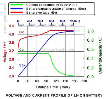
When the cell is given Constant voltage, the cell absorbs the constant^ current during charging. The cell can absorb as much current as it is given, but providing current more than rated value could reduce battery life or heat up quickly to damage the cell (check the datasheet for rated charging current).
^ almost constant during 20{42041a7992ac3be9e9e29c856254fb498d8c7935d7cf8512da6802e8688e734a} to 90{42041a7992ac3be9e9e29c856254fb498d8c7935d7cf8512da6802e8688e734a} of the state of charge, for more information, check the state of charge of lithium battery
Charging voltage:
The standard constant charging voltage varies from manufacturer to manufacturer but does not vary much, as it changes as 4.2V, 4.3V, and 4.4V. These are safe values, you can even charge with little higher voltages.
(You can also use 5V to charge 18650 cells. This will not damage the cell if you don’t allow it to overcharge, by terminating the charging and preventing damage to the cell after the li-ion cell reached 4.2 volts.) A standard charging value on the typical datasheet is generally mentioned at 0.5 C, where C stands for capacity. So the practical value of the charging current must be equal to or less than half the battery capacity mentioned.
For example, in a 1700 mAh cell, the standard charge current would be 850 mA, and for a 2400 mAh cell, the standard charge current would be 1200 mA.
It is recommended to keep the charging current at or below the limit specified in the datasheet.
(check 18650 battery specification and datasheet here)
When the battery voltage reaches 4.1 V or 4.2 V, the 18650 battery cell is almost fully charged. This may be called as 18650 battery charging voltage. From this moment, the current consumed by the battery starts decreasing steadily to reach a certain value*.
Charge termination:
When the current drops below or stays at a certain value*, charging should be terminated. The most commonly practiced charge current termination limits are between C/10 and C/30.
For example, in a 1700 mAh cell, the standard charge current would be 850 mA. Thus the charge termination current will be near 85mA and
For a 2400 mAh cell, the standard charge current would be 1200 mA, thus the charge termination current will be near 120mA.
Important before charging using methods mentioned on this page:
When the battery is fully charged means reached charge current termination value, the battery should be disconnected immediately from the power source.If the battery is kept connected to the dc power source will cause the battery to overcharge and eventually it will swell, resulting in damage to the battery. *check datasheet, click here for sample 18650 datasheet.
To avoid damage to the cell, use 18650 chargers with overcharge, over-current, over-voltage protection features. So you can rest assured of safety to the battery.
Charging the 18650 battery without a charge controller (like tp4056, tp5100 etc.) is not advised due to the risk of overcharging and damages.
Charging the 18650 battery without a charger is possible with the proper knowledge, precaution, and method we have shown below.
If you are charging the 18650 battery without a charger then charge 1 cell at a time with the information given in the theory part above.
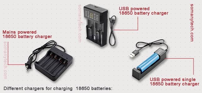
Charging with 18650 battery charger:
Use the charger shown in the image above, available for sale online on Amazon or eBay.
This is the simplest and best method to charge 18650 battery without concerning about the removal of the battery from the charger to protect it from overcharging, over-voltage, or short-circuit.
These chargers have an inbuilt over charging protection circuit and cut-off circuit that disconnects the battery when it is fully charged, which ensures the long life of the battery and performance.
It also comes with battery charging state display/ indicators, their function may vary from charger to charger.
There are two types of 18650 lithium-ion battery chargers available in the market:
USB powered 18650 battery chargers: With these chargers, you can charge the battery from any USB power port/socket you see around. It is recommended to use your high current rated mobile charger to charge batteries with this device.
Otherwise, it will slow-charge the batteries or you can say slow charging. The good thing about this device it is highly portable you can carry it along traveling and use it with any type of USB port.
Mains power 18650 battery chargers: In this, you can directly connect the charger with a mains power supply that is available at your home. They could charge faster than USB-powered chargers.
How to charge 18650 battery using tp4056?
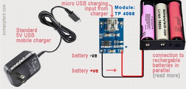
Component required: connecting wires, 18650 battery holder, tp4056 module, 5v mobile charger 1.0 Amp or more.
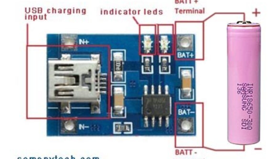
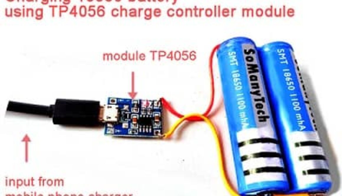
It’s very easy to use the tp4056 module. There is need to identify 2 terminals on the board viz. BAT+, BAT- only. Just connect the positive terminal of the battery to the BAT+ on the board and the negative terminal of the battery to the BAT- on the board as shown in the image below.
Component required: 5V mobile phone charger (1Amps or more), connecting wires, 18650 battery holder, tp4056 module(required).
By doing connection shown in the above image, you can charge 18650 battery safely. If you are using low current rated mobile phone charger then charge only one 18650 lithium cell with it. As more cells will draw more current that can goes up more than 1 ampere, so there is a chance that your charger would heat up very quickly and get permanently damage.
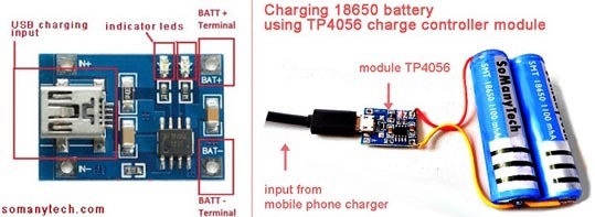
This above image shown the detail of the terminals of tp4056 and final setup of 18650 charging circuit without cell holder.
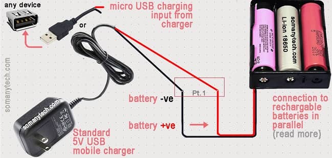
8650 battery charger using old phone charger or USB port
Component required: 5V mobile phone charger(capacity of 500mA or more), connecting wires, 18650 battery holder, tp4056 module(optional).
Connect the circuit as shown in the above circuit, keep checking output voltage of the battery using a multimeter (charger disconnected) to read voltage of 4.2 volts.Remove battery at 4.1 volts, its recommended if you are not using any charge controller. (read theory above for safe operation)
You can also charge 18650 battery using USB i.e, the output of USB port for charging. Use only one cell at a time.(connect charge controller module at ‘pt.1’ if possible for safe operation)
How to charge 18650 battery without charger?
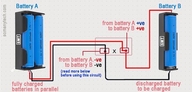
Direct charge using fully charged 18650 battery:
This method could be rarely used for charging purposes, as it just shares power from the ‘fully charged battery’ to ‘discharged battery’. What if you don’t have any type of device or power source to charge a 18650 battery? then you can use this method to charge a completely discharged battery.
Connect the circuit as shown in the above circuit for about 30 to 60 minutes. The completely discharged battery will acquire some charge from fully charged batteries. (connect charge controller module at ‘X’ if possible for safe operation)
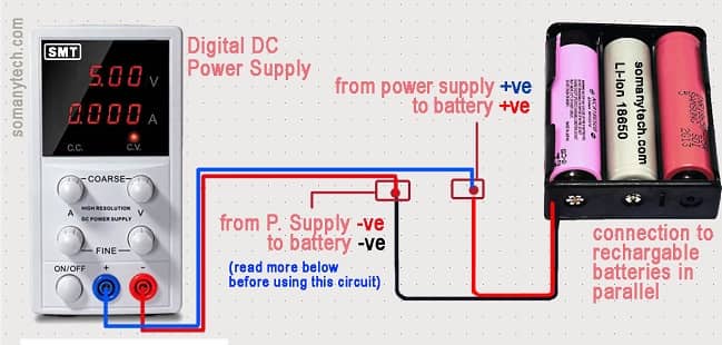
18650 battery charger using bench DC power source (without charger)
You can charge a 18650 battery without charger if a DC bench power supply is available with you, but it is quite an unconventional method. It is to be used attentively while charging batteries with a bench DC power supply. Note that if you are not Experienced in electronics core electrical circuits and its rules, then avoid trying this!! if you overcharge or connect Lithium batteries in Reverse polarity, they may bulge or catch fire. It is recommended to charge one battery at a time, following steps and calculation values for one 18650 battery at a time.
Step1: Make sure that the power supply output voltage is at 4.3V before connecting to the battery.
Step2: Turn off the bench DC power supply from mains as well as from the bench unit before connecting wires.
Step3: Properly connect the positive terminal of the batteries to the positive terminal of the DC power supply, and connect the negative terminal of the battery to the terminal of the DC power supply. Make sure that connections are tight (not loose).
Step3: Turn on the switch & ensure 4.3v at the output.
Now monitor the reading of bench power supply according to the already discussed points in the theory part.
Here, (for single-cell) the initial current would be more than 400mA while charging. Disconnect the batteries when the current consumption ranges from 25 to 100mA (depends on battery capacity). This means that your battery is almost charged.
If you do not want to monitor and disconnect the battery manually then you can use a charge controller module like TP 4056. The charge controller will automatically control the current to the batteries and disconnect when fully charged. Also, it is safe!!
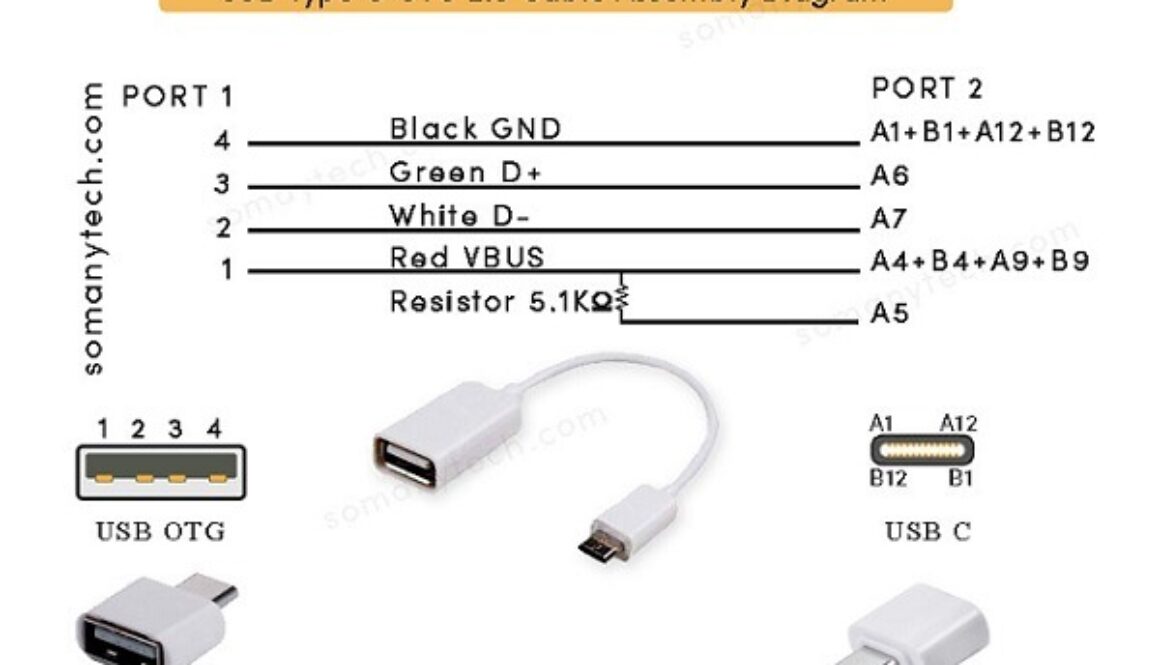
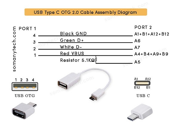
The USB C OTG wiring diagram below shows the “ USB type C to USB A female 2.0 type cable assembly”:
Before discussing the USB C OTG wiring diagram: Let’s lake a brief overview an OTG cable, or OTG connector.
An OTG C or On The Go adapter enable you to connect a full sized USB pen-drive or USB A cable to your phone through the Micro USB-C charging port.
They can be purchased separately from retailers, as they don’t come with a box in general when you purchase any device. The main purpose of USB-C OTG is a transfer of data with pen-drives as well as enable connectivity to peripherals like mouse and keyboard.
The USB Type-C cable, receptacle, and plug are designed to be more sturdy and user-friendly than existing USB cables namely Type-A and micro USB Type-B.
Let’s take an example, Type-A plugs connect only in one position to a Type-A receptacle (female port). The Type-C connector, however, lets you connect the device downside up or upside down. By making this simple change, USB devices can be inserted correctly into USB ports without frustration.
USB C 2.0 OTG (OTG) product is a portable device, that can function either as a USB host or a USB peripheral. All USB 2.0/ 3.0 OTG products are required to use a micro-B/micro-C receptacle.
Fig. shows the receptacle pin assignment for supporting a semi-featured Type-C cable. A full-featured cable supports both USB 2.0 and USB 3.1 (higher data speed). Below is the USB Type C 2.0 OTG wiring connection USB A to USB C:
Table 1 shows the pin-out for both receptacle and plug of USB OTG.
USB A receptacle
USB C port
Wire code
Description
Symbol
1
A4, B4, A9, B9
Red
+5V (dc power)
VCC/ VBUS
2
A7
White
Data- (data from device to host)
D-
3
A6
Green
Data+ (data from host to device)
D+
4
A1, B1, A12, B12
Black
0V (dc ground)
GND
NC
A5*
-
Configuration Channel 1 (VBUS through resistance Rp =5.1kΩ)
CC1
Description:
The OTG device functions as a USB peripheral. When acting as a USB peripheral, the portable USB 2.0 OTG product observe VBUS signal to determine whether it is connected to a USB host or external mobile charger.
The Pin no A1, A12, B1, B12, of USB C port is connected to the Pin no.4 USB type A receptacle. This pin is named as the ground (GND) through that pin ground signal is established.
The Pin no A4, A9, B4, B9, of USB C male is connected to Pin no.1 from USB type A receptacle male. This pin is the power supply (5+ volt/ VBUS) through that pin the power is supplied to the device and it can be host or peripherals.
The Pin no. A6 of the C- port is connected to Pin no.3 from USB type A receptacle.
Also, the Pin no. A7 of micro USB C is connected to the Pin no.2 from USB type A female.Pin no. 2/A7 (D-) and pin no. 3/A6 (D+) both as a pair are used as a differential data pin in each port.
USB 3.X attained its massive speed increase with the addition of 5 more wires containing 2 pairs, one each for TX and RX (viz, TX+/ TX-, RX-, RX+), and an additional ground return.
The creative part is how to identify additional 5 connections, thus allocating new USB C wire color codes to the wires other than existing USB 2.0 wires.
USB 2.0 and 3.0 “type A” connectors are interchangeable and compatible, the extra 5 pins added such a way that there should be no compatibility issues.
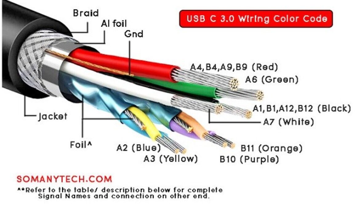
Below image showing USB C type C cable color code showing signal name at USB C plug:
^ Blue colored Mylar material Foil with conducting inner layer/ separate connector is optional and may not present in some wires also its presence does not disobey the USB protocol either, these are independent ground but connected at end.
*All signal names viewing at USB type C plug end and USB C wires inside.
You could be interested in USB C 2.0 & 3.0 pinout and their detailed function, do check here -> USB C pinout for 2.o and 3.0
USB type c wire color table/ port USB C color code :
Conductor Color
Pins At Port
Signal Name
RED
A4,B4,A9,B9
VBUS
WHITE
A7
Dn1/ D-
GREEN
A6
Dp1/ D+
BLACK
A1,B1,A12,B12
GND
N/A
A5
CC
N/A
B5
VCON
BLUE
A3
TX1-
YELLOW
A2
TX1+
PURPLE
B10
RX1-
N/A
GND
GND
ORANGE
B11
RX1+
N/A
SHELL
SHIELD
A6 and A7 are differential Data lines. They are used as Data lines (D+ & D-) for USB 2.0 connections only. A6 and A7 are usually un-shielded pair of wires, in which A6 is Green in color, and the color of A7 is white.
A4+B4+A9+B9 (VBUS) is an individual wire for power supply. Its color code is red and all these pins are common at terminal end. A1,B1,A12,B12 (GND) is an individual wire for power supply. Its color code is black and all these pins are common at terminal end.
(B10+B11) are shielded pair of high speed data receive signal (RX1- & RX1+), in which B10 is coded as purple and B11 is coded as orange.
They are shielded with conducting foil generally made of aluminum material. If there is extra conductor along with this pair it is a ground.
(A2+A3) are shielded pair of high speed data transmit signal (TX1- & TX1+), in which A2 is coded as blue and A3 is coded as yellow.
They are also shielded with conducting foil generally made of aluminum material. If there is extra conductor along with this pair it is a ground. The shield is individually grounded at both ends.
Note that the mention color code above is as per USB C standards, there may be some cable that don’t have exact same color of wiring. Some manufacture may have different color of wires in the USB type C cables.
Generally, Vbus/ Gnd /D+ /D- have fixed color code and followed by most manufacture, other signals may have different pattern like in color combination.
Few example are: (TX1+ TX1-) & (RX1+ RX1-) could be of black and white color but in different color jacket/ Mylar foil.
The USB implementer Forum sets the standards for data transfer through various cables and connectors one can use on the end of those cables, that also includes USB communication protocols. This post will take you to the USB C wiring diagram/ USB C 3.0 wiring diagram and related information in detail.
USB 3.1 Gen 1 which is formerly known as USB 3.0, later renamed USB 3.2 Gen 1×1 port.
This means that USB 3.0 is the same as USB 3.1 Gen 1.
Also, USB 3.1 Gen 1 is the same as USB 3.2 Gen 1×1.
This can be concluded that all USB 3.0/ USB 3.1 Gen1/ USB 3.2 Gen 1×1 are having same hardware interface and USB protocol. All new generation USB 3.x are made backward compatible to USB 3.0 and 2.0; USB Type-C to USB-A Male 3.1/ 3.2 Gen2 Adapter charger cable supports data transfer rate upto 10Gbps
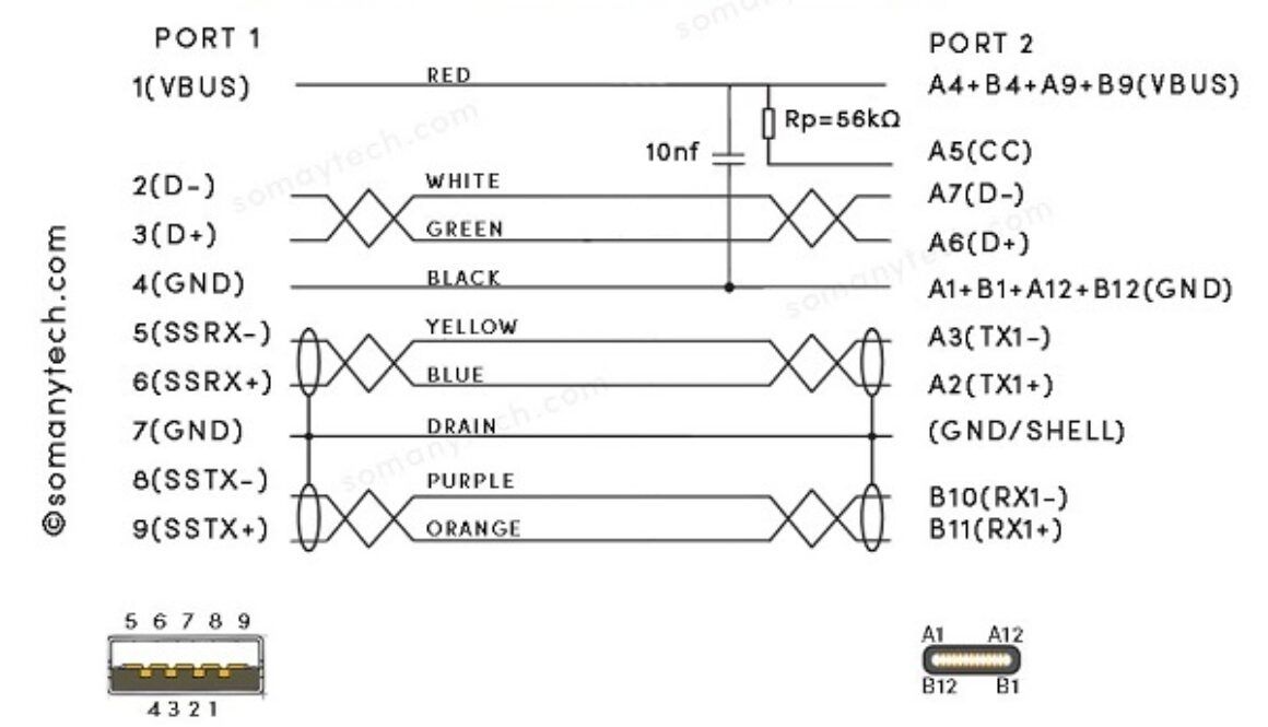
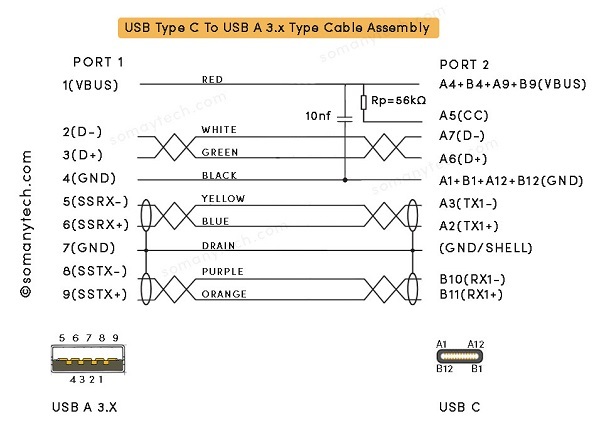
USB C wiring diagram to male USB 3.1/ 3.2 type A Gen1/ Gen2:
As you know that USB C 3.x is made to be operated reversibly, also by looking at pin out diagram of USB c male you can see that all the pins termed A could be interchangeably used with that of termed B. check USB Type C 3.0 pinout!!
The table shows below the connection between pins on both the end of the plugs and their functions with respective symbols:
Signal Name
Port 1
Conductor Color
Port 2
Signal Name
VBUS
1
RED
A4,B4,A9,B9
VBUS
D-
2
WHITE
A7
Dn1/ D-
D+
3
GREEN
A6
Dp1/ D+
GND_DRAIN
4
BLACK
A1,B1,A12,B12
GND
N/A
-
N/A
A5
CC
N/A
-
N/A
B5
VCON
SSRX-
5
BLUE
A3
TX1-
SSRX+
6
YELLOW
A2
TX1+
SSTX-
8
PURPLE
B10
RX1-
GND_DRAIN
7
-
GND
GND
SSTX+
9
ORANGE
B11
RX1+
SHIELD
SHELL
N/A
SHELL
SHIELD
According to the USB standard, VBUS carries a +5v and the default output current of up to 3.0A.
Pin no.1 from USB type A 3.1 male is connected to the Pin no A4, A9, B4, B9, of USB type C. This pin is named as the (+VDD/ VBUS) through which the power is supplied to the device or any equipment which is also an indicator of handshake signal, that convey the system that “the device is connected”.
Pin no.4 from (Port1) USB type A 3.1 male is connected to the Pin no A1, A12, B1, B12, of (Port2) USB-C. This pin is the ground return (GND). This is individual black color wire.
Pin no.3 from USB 3.1 type A male is connected to the Pin no. A6 of port 2.
Pin no.2 from USB type A male is connected to the Pin no. A7 of port 2.Both Pin no. 2/A7 (D-) and pin no. 3/A6 (D+) are used as a differential data pin in each port. Data is sent from and received from these port when used in USB 2.0 mode (in reverse compatibility mode with previous generation USB host)
Pin 7 is connected as a Drain/Shell.
Pin no. 5 (SSRX-) from port 1 is connected to Pin no. A3 (TX1-) of port 2, Pin no. 5 (SSRX+) from port 1 is connected to Pin no. A3 (TX1+) of port 2.
SSTX are bidirectional data SuperSpeed Transmitter ends.
Please note that SSRXp1 can be written as SSRX1+, also SSRXn1 can be written as SSRX1-
Pin no. 8 (SSRX-) from port 1 is connected to Pin no. B10 (RX1-) of port 2, Pin no. 9 (SSRX+) from port 1 is connected to Pin no. B11 (RX1+) of port 2.
SSRX are bidirectional data SuperSpeed Transmitter ends.
Please note that SSTXp1 can be written as SSTX1+, also SSTXn1 can be written as SSTX1-
USB type C terminologies and parameters for technical/ manufacturing use:
Pull-up resistor (Rp): The pin A5 /(CC) is connected in series with resistor Rp= 56kΩ with the +5v (VBUS) at USB C plug terminal. The value of Rp determines the current sourcing capability of the Type-C ports for which it is designed.
SHELL/ SHIELD/ BRAID: For a good quality USB cable, to avoid crosstalk and RF interference from adjacent data lines, it is recommended to have 360-degree conductive shielding with ground shield termination on both ports.
The main purpose of shielding is to prevent unwanted RF interference and noise signals.
In common practice, A6 and A7 are un-shielded pair of wires, (B10+B11) and (A2+A3) are shielded pairs of wires respectively, shield is individually grounded at both end, remaining ground connection should be individual black color conductor. Also check different USB mode here
IC LM2596 HV could be an alternative to LM 2596 dc to dc buck converter IC, if later is not available. Thus you can use an IC LM2596 HV dc to dc buck converter for the same purpose. Other than HV i.e, higher voltage operations, it has very similar working and specifications.
The LM2596 HV is a popular voltage regulator/ buck converter IC ideally suited for convenient design of a step−down or you can say step-up switching regulator. It is capable of driving a total load of 3.0 Amps with excellent line and load regulation.
In addition to the 3.3V, 5V, and 12V output version, this power converter has an adjustable output version as well.
In comparison with popular three-terminal linear regulators, the LM2596 HV buck converter is significantly more efficient due to its switch-mode power supply feature, especially when input voltage is high.
The LM2596 HV operates at a higher switching frequency of 150 kHz, which means smaller sized filter capacitors would be needed as compared to lower frequency switching regulators.
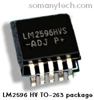
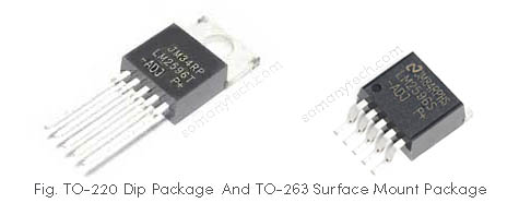
If talking of packaging, it is available in a standard 5−lead TO−220 package with several different lead bend options (check datasheet), the TO-263 D2PAK surface mount package and a SOP-8 surface mount package
Some of the main features include a maximum ±4{42041a7992ac3be9e9e29c856254fb498d8c7935d7cf8512da6802e8688e734a} tolerance at output terminals when conditions are as specified, (when input voltage and load conditions are met).
It is Available in a fixed 3.3V, 5V, 12V and an adjustable output voltage range of 1.20 V − 57 V.
Maximum of 3.0 A output load current.
Available in TO-220, TO-263 and SOP-8 packages.
Wide input voltage range up to 60 Volts.
A 150 kHz fixed frequency internal oscillator.
Requires only 4 external components.
TTL shutdown capability (for digital/ analog ON/OFF)
Low power standby mode – consumes as low as 30 uA when in standby.
Built-in thermal shutdown and current limit.
Schematic diagram of LM2596 HV dc to dc buck converter module:
Components required:
IC 2596 HV ADJ TO-220 dip package with heatsink, L1 = inductor = 68uH, R1 = 5kΩ, R2 = variable resistor 100kΩ or higher, C1 = 470uF 63V, C2 = 470uF 63V, Schottky switching diode = IN5822 (any alternative will work).
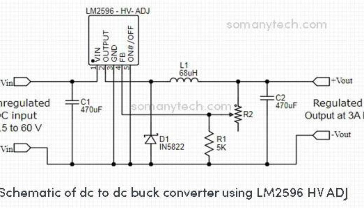
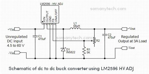
Check below circuit diagram for adjustable dc to dc buck converter using LM 2596 HV ADJ version of the IC.
The above image clearly shows the circuit connections/ wiring diagram. Please ensure that the input voltage must be (1.5 volts) higher than the required output voltage. Make sure to follow the “Circuit Design Rules” when implementing a PCB (printed circuit board) design.
In general, input could be between 4.5V and 60V. And the output could be derived in the range of 1.20V to 57V, and maximum up to 3 Amps.
The output of the circuit is determined by the FB (feedback voltage). We just needed to add resistor R1 and R2 to the feedback pin(4) as shown in the circuit diagram. The feedback voltage depends on the value of resistor R1 and R2. Thus, by adding a variable resistor, you can control the output voltage according to the following equation:
Vout = Vref(1+R2/R1)
Where, Vref= 1.23 Volts
And, R1 could be between 1KΩ to 5KΩ, choose R2 be a variable resistor.
Also check, 3.7v to 5v Boost Converter Circuit
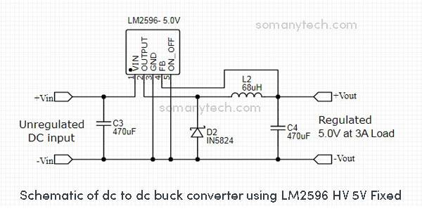
Capacitors C1 and C3 are input filters that stabilize changes in DC input. Also, capacitors C2 and C4 are output filter capacitors.
If you are working on wide range input and output voltages. Then you must select the output capacitor accordingly (voltage ratings must be higher than that of operating voltage range, in this case 63V rated capacitors).
Choose capacitor values as shown on this post or recommended in the data sheets of respective ICs.
Check below circuit diagram for dc to dc buck converter using fixed version of the LM2596HV.
This is a 5v fixed version of the IC, you can use 3.3V and 12V versions of IC as well in the above circuit. (schematic would be same for all fixed version of LM2596 HV IC)
Pinout diagram of LM2596 HV:
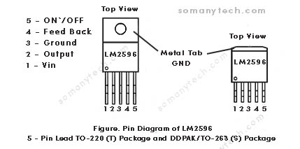
There are five total pins on the LM2596 HV, TO-220 and TO-263, as follows:
Pin(1)= Input voltage pin= This pin connects the input supply with the input filter capacitor to prevent voltage spikes at input.
Pin(2)= Output pin (circuit is different for fixed regulators and Adj. version)
Pin(3)= Ground pin = This pin is connected to the ground and a heatsink.
Pin(4)= Feedback pin = This pin returns feedback voltage to the internal comparators for regulation.
Pin(5)= ON/OFF = It is a negative trigger terminal, this means grounding (0 volts) will enable and 1.3 V or higher volts will disable the operations of the internal circuit. This pin is used to standby the voltage regulator circuit to current consumption as low as 30uA.
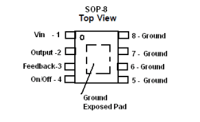
There are eight total pins on the LM2596 HV, SOP-8 package, as follows:
Pin(5), Pin(6), Pin(7), Pin(8) = Gnd =This pin is connected to the supply ground.
Pin(1)= Vin = This pin is connected with unregulated input voltage.
Pin(2)= Vo = Required output is taken from this terminal.
Pin(3)= Fb= Feedback voltage is given to this terminal.
Pin(4)= On/Off = Enable or disable the regulator IC.
Applications of LM2596 HV series:
In the power supply circuits of li-ion battery chargers.
Any type of load that takes upto 3 Amperes.
Any devices where high efficiency step−down or step-up regulators are required.
Can be used as a high efficiency pre−regulator for better Linear Regulation.
(All the datasheets and IC’s nomenclature ownership belongs to the respective semiconductor company. The purpose of this post is to elaborate the applications of popular voltage regulators)
The LM2596 is a popular voltage regulator/ buck converter IC ideally suited for convenient design of a step−down, or you can say step-up switching regulator. With excellent line and load regulation, it can drive a total 3.0 Amps of load.
These power converters are available in fixed output voltages of 3.3V, 5V, 12V, and an adjustable output. The device with an adjustable output version is internally compensated to minimize the number of external components to simplify the power supply design circuits.
In comparison with popular three-terminal linear regulators, the LM2596 buck converter is significantly more efficient due to its switch-mode power supply feature, especially when input voltage is high.
The LM2596 operates at a higher switching frequency of 150 kHz, which means smaller sized filter capacitors would be needed as compared to lower frequency switching regulators. If talking of packaging, it is available in a standard 5−lead TO−220 package with several lead bend options (check datasheet), and the D2PAK surface mount package.
Note: IC CA2596 could be an alternative to LM 2596 dc to dc buck converter IC, if later is not available. Thus, you can use an IC CA2596 dc to dc buck converter for the same purpose. It has very similar working and specifications, you can use the below-mentioned schematic for CA2596 or refer to the datasheet for details.
The main features include a max of ±4{42041a7992ac3be9e9e29c856254fb498d8c7935d7cf8512da6802e8688e734a} tolerance at output terminals when specified input voltages and load conditions are met. External pin(5) is implemented to ON/OFF the power converter.
Available in a fixed 3.3V, 5V, 12V and an adjustable output voltage range of 1.23 V − 37 V.
Maximum of 3.0 A output load current guaranteed.
Available in TO-220 and TO-263 packages.
Wide input voltage range up to 40 Volts.
A 150 kHz fixed frequency internal oscillator.
It requires only 4 external components.
TTL shutdown capability (for digital/ analog ON/OFF)
Low power standby mode, as low as 80 uA when in standby mode.
Internal thermal shutdown and current limit protection.
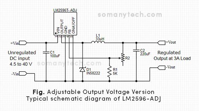
Schematic diagram of LM2596 dc to dc buck converter module:
Components required: IC 2596 TO-220 dip package with heatsink, L1 = inductor = 33uH, R1 = 5kΩ, R2 = variable resistor 100kΩ or higher, C1 = 100uF 50V, C2 = 220uF 50V, Schottky stitching diode = IN5822 (any alternative will work).
Check below circuit diagram for adjustable dc to dc buck converter using LM 2596 ADJ schematic of the IC.
The above image is self-explanatory in terms of wiring diagram/ circuit connections. Please ensure that the input voltage must be (1.5 volts) higher than the required output voltage. Also follow ‘Circuit Design Rules’ while implementing a PCB (printed circuit board) design.
In the general, input could be between 4.5V and 40V. And the output could be derived in the range of 1.23V to 35V, and maximum up to 3 Amps.
The output of the circuit depends on the FB (feedback voltage). We just needed to add R1 and R2 to the feedback pin(4) as shown in the schematic. The feedback voltage is dependent on the value of resistor R1 and R2. Thus, to make the output voltage controllable add a variable resistor and get the desired voltage according to the following formula:
Vout = Vref(1+R2/R1)
Where, Vref= 1.23 Volts
And, R1 could be between 1KΩ to 5KΩ, choose R2 be a variable resistor.
The capacitor C1/C3 are input filter capacitor that stabilize change in DC input going to the IC. Also, capacitor C2/C4 are output filter capacitors.
If you are working on full range input and output voltages. Then you must choose output capacitor accordingly (voltage ratings must be higher than that of operating voltage range).
Also choose capacitor value as shown on this post or that of recommended in datasheets of respective IC.
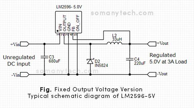
Check below circuit diagram for dc to dc buck converter using fixed version of the IC.
This is a 5v fixed version of the IC, you can use 3.3V and 12V version of IC as well in the above circuit. (schematic would be same for all fixed version of LM2596 IC)
Pinout diagram of LM2596:
There are five total pins on the LM2596, as follows:
Pin(1)= Input voltage pin= This pin connects the input supply with the input filter capacitor to prevent voltage spikes at input.
Pin(2)= Output pin (circuit is different for fixed regulators and Adj. version)
Pin(3)= Ground pin = This pin is connected to the ground and a heatsink.
Pin(4)= Feedback pin = This pin returns feedback voltage to the internal comparators for regulation.
Pin(5)= ON/OFF = It is a negative trigger terminal, this means grounding (0 volts) will enable and 1.3 V or higher volts will disable the operations of the internal circuit. This pin is used to standby the voltage regulator circuit to current consumption as low as 80uA.
Applications of LM2596 buck converter:
In power supply circuits of lithium-ion battery chargers
Any type of load that takes 3 Amperes of current.
Simple applications where high efficiency step−down or step-up regulators are required.
Can be used as a high efficiency pre−regulator for Linear Regulators.
Negative Step−Up Converters.
LM2596 Datasheet :
For more detailed technical information on this power converter, check lm2596 IC datasheet here. (All the datasheets and IC’s nomenclature ownership belongs to the respective semiconductor company. The purpose of this post is to elaborate the applications of popular voltage regulators)
If are you looking for a way to power your 9V projects using a 12V power source or a 12v battery then, below is a schematics of the simple 12V to 9V converter circuits. With the right components and some basic knowledge of electronics, you can build your own converter that will step down the voltage from 12V to 9V. These converter circuits designed to use with any micro-controller, modules or any IC’s. Here we mainly use reliable linear power converters like LM7809 and LM317.
In this article, we will provide you an overview of the basic functioning of voltage conversion and guide you through the steps of building a simple 12V to 9V converter circuit.
12v to 9v converter with LM7809:
LM7809 is a fixed voltage regulator IC that reduces and regulates the input voltage in electrical circuits. A voltage regulator 12v to 9v converter with IC LM7809 is implemented as shown in the schematic diagram below. It can be used for low current application as well as for the current up to 2 Amp or more.
Note that, you have to use the input capacitor ‘Cin’ and an output capacitor ‘Co’ to the IC 7809. The heat sink is necessary because the voltage-drop of 3 volts is to be dissipated as heat. There is a possibility of IC being destroyed if the heat-sink is not connected. The input-output voltage difference here is 3volts which is more than the recommended value of 2.5Volts.
Components required: A 12v battery/ 12V adopter supply, 100uF capacitor, 0.1uF capacitor, IC LM7809, a Heat-sink, wires, and connectors.
Working:
The IC has a lot of built-in features like thermal shutdown, short circuit protection, and safe operating area protection. LM7809 is an IC of LM78xx series all the ICs in this series are made for different fixed output voltages. These types of ICs are commonly used in regulated power supply circuits.
LM7809 a linear transformer IC. The digits ‘xx‘ represents the value of the o/p regulated volts. The 7809 IC gives 9V DC as the digit ‘xx‘ in last represents (09). Pin 1 is the input pin. Pin 2 is the ground pin. Pin 3 is the output pin.
LM317 12v to 9v converter:
A 12v to 9v dc converter can also be made with a versatile IC LM317 linear voltage regulator. It is useful for medium to high current circuits (1 Ampere to 1.5 ampere+) with the proper heat-sink.
Generally, LM317 is found at variable power supply circuits that give regulated voltage (1.25V to 37V) on changing the voltage on pin no.1. Here, the voltage divider circuit is used with LM317 gives a fixed o/p of 9v.
Important: It is insisted to add an input capacitor Cin (also the o/p capacitor Co). A heat-sink is a must to cool down the IC from the heat generated inside the IC. The i/p voltage must be at least 1.5V greater than the rated output voltage for this IC to be operated as described.
Components required: A 12v battery/ 12V power source, a 2.2k ohm resistor, 300-ohm resistor 100uF capacitor, 0.1uF capacitor, IC LM317, a Heat-sink.
Working: The LM317 is an adjustable voltage regulator IC competent of supplying more than …
12v to 9v converter using resistors as a voltage divider:
The schematic below shown below is the circuit for low current (~20 mA) applications, or to take reference voltage in comparator circuit or low current drawing circuit of an LED. You can drive three LEDs in series across the o/p of R2 resistor if you are using a 12volt battery in the input end.
This type of circuit is not efficient circuits, thus not recommended for use in project circuits.
Components required:
One 12v battery, 300-ohm resistor, 1k resistor, some wires. It is just a voltage-divider circuit. You can obtain the output according to your need with this formula:
Where, Vo is the o/p voltage. Vin is the source voltage. Pick any resistor value either R1 or R2 (also depends on load impedance) and solve for other. Then choose the nearest std. value of the resistor.
12v to 9v converter using zener diode:
The circuit shown below zener voltage regulator schematic, it is useful for (1-900mA) medium current drawing circuit eg. LED indicators, transistor switches, Arduino, etc
Use this 12v to 9v converter (DC to DC) circuit with any other circuit across the 9.1v zener diode. You will get about 9.1V at the output.
Important: The load must be connected to the output end to prevent zener from getting damaged.
Series resistor 10 ohm is a current limiting resistor and when high current is drawn it has to pass that current through it, thus 5-watt resistor is necessary.
Components required: A 12v battery, 10-ohm resistor (≥10 ohms), 9.1V zener diode (5W), some wires or connectors.
Working: It is the most common circuit of zener diode in voltage regulator configuration. Design 9volt zener voltage regulator from a 12volt power supply source. The maximum power rating …
For detail calculation and formulae search for 9v to 5v converter article on this website.
Simple 12 Volt to 9 Volt DC-DC Converter using transistor:
These types of schematics are outdated but still found in several peripherals. This is the transistor- zener voltage regulator in EC mode: