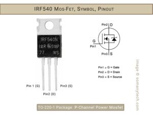
For the high-current switching application, the IRF540 MOSFET is one of the popular choice. The IRF540 stands out for its fast switching, rugged device design, low on resistance and cost-effectiveness.
In this article, we have discussed IRF540, check its pinout, equivalent, practical applications, distinctive features, as well as instruction on when and where to employ this high-current N-channel MOSFET.
Main Features:
Maximum Rated voltage across Drain & Source → Vdss=100V
Maximum operating current → Id = upto 28Amps
Gate voltage → VGS(th) = 2V to 4V
Resistance → R(DS)(on)= 77.0 mΩ or 0.077 Ω
Primary function → High current high speed switching.
Parameter overview:
The IRF540 MOSFET is designed for high-current application, having a remarkable 100 Volt drain-to-source voltage limit. Its gate trigger voltage, starting from up to 4V, making it suited to a low-voltage switching control applications as well. As a result of its exceptionally low drain-to-source resistance, the device has an operating current capacity of 100 Amp. With industry standard footprints, this device is available in surface mount and through-hole packages for ease of design.
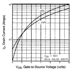
The below plot showing Typical Transfer Characteristics of MosFet:
-Id (Vs) -Vgs, @ Vds=50V, Pulsed Drain current @20µs with junction temperature maintained at 25°C and 175°C. It can be observed that this MOSFET can be used at as low as 2V-4V for lower current application of up to 5Amp. But for higher Load. Current you need to drive the gate with an appropriate voltage (Vgs) ensuring guaranteed optimal switching performance.
For detail characteristic like Temp. vs Id, Vds vs Ids, check and refer to the IRF540 Datasheet below.
When working with the MOSFET IRF540 circuit, it’s essential to follow recommended practices, including:
Review the datasheet for detailed electrical characteristics and guidelines, especially when implementing N-channel applications. And ensure proper heat sinking to dissipate any generated heat effectively.
Application/ Uses:
High ruggedness and current capability make it an industry-standard choice. Widely available through distribution partners, ideal for 50W applications and drop-in replacements due to standard pinout.
Some of the application of IRF540 are: DC motors in reverse direction, inverters, SMPS (Switched-Mode Power Supplies), lighting systems, load switches, and even battery-powered devices, reverse polarity protection.
Alternatives & Replacement for IRF450 are: IRF3205, IRFB7440, CJ340, etc
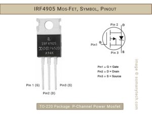
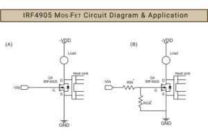
In need of high-current switching application, the IRF4905 MOSFET is one of the preferred choice. The IRF4905 stands out for its reliability and efficiency, making it the preferred selection for applications requiring rapid switching speeds and the power control system.
In this article, we have discussed IRF4905, check its pinout, equivalent, practical applications, distinctive features, as well as instruction on when and where to employ this high-current P-channel MOSFET.
Main Features:
Maximum Rated voltage across Drain & Source → Vdss= -55V
Maximum operating current → Id = upto -74 Amps
Gate voltage → VGS(th) = -2V to -4V and lower
Resistance → R(DS)(on)= 20.0 mΩ or 0.02 Ω
Primary function → High current high speed switching.
Parameter overview:
The IRF4905 MOSFET is designed for high-current application, having a remarkable -55 Volt drain-to-source voltage limit. Its gate trigger voltage, starting from -2 volts up to -20V, making it suited to a low-voltage switching control applications as well. As a result of its exceptionally low drain-to-source resistance, the device has an operating current capacity of -79 Amp. With industry standard footprints, this device is available in surface mount and through-hole packages for ease of design.
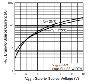
The below plot showing Typical Transfer Characteristics of MosFet:
-Id (Vs) -Vgs, @ Vds=-25V, Pulsed Drain current @20µs with junction temperature maintained at 25°C and 175°C. It can be observed that this MOSFET can be used at as low as negative 2V-4V for lower current application of up to 5Amp. But for higher Load
Current you need to drive the gate with an appropriate voltage (-Vgs) ensuring guaranteed optimal switching performance.
For detail characteristic like Temp. vs Id, Vds vs Ids, check and refer to the IRF3205 Datasheet below.
When working with the MOSFET IRF4905 circuit, it’s essential to follow recommended practices, including:
Review the datasheet for detailed electrical characteristics and guidelines, especially when implementing P-channel applications. And ensure proper heat sinking to dissipate any generated heat effectively.
Application/ Uses:
High ruggedness and current capability make it an industry-standard choice. Widely available through distribution partners, ideal for low-frequency applications <100kHz and drop-in replacements due to standard pinout.
Some of the application of IRF4905 are: DC motors in reverse direction, inverters, SMPS (Switched-Mode Power Supplies), lighting systems, load switches, and even battery-powered devices, reverse polarity protection.
Alternatives & Replacement for IRF4950 are: IRF9540, IRFB7440, CJ340, etc
In high-current switching scenarios, the IRFZ44N MOSFET is a well-regarded choice. Such powerful transistors play crucial roles in various applications, including device and motor control. The IRF3205 is known for its durability and efficiency, making it a preferred option for tasks requiring very high speed switching and handling high power. Thus, comprehending the features and capabilities of this transistor is significant.
In this article, we’ll explore the IRFZ44N, including its pinout, equivalent components, practical uses, features, and how and where to use this high-current N-channel MOSFET.
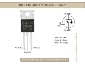
The IRFZ44N, made by International Rectifier, is easily recognized by its part number prefix. It boasts low on-resistance, fast switching, and efficient HEXFET power MOSFET design, making it suitable for various commercial and industrial applications with power dissipation needs of up to around 50 watts, preferred TO-220 package.
Main Features:
Maximum Rated voltage across Drain & Source → Vdss= upto 55V
Maximum operating current → Id = upto 49 Amps
Gate voltage → VGS(th) = 2V – 4V and above
Resistance → R(DS)(on)= 17.50 mΩ
Primary function → High current high speed switching.
Parameter overview: The IRFZ44N MOSFET is designed for high-power applications, with the ability to handle a drain-to-source voltage of up to 55 volts. Additionally, it can be triggered with a minimal gate voltage ranging from 2 to 4 volts and above it could be used, making it suitable for low-voltage control. Its maximum operating current of 49 amps is achieved thanks to its exceptionally low drain-to-source resistance of 17.5 milli-Ohms.
Package
TO-220
Transistor
Component
N-Channel
MOSFET
Drain to Source Voltage
55v
Max.
Continues Drain Current
49A
Max.
Voltage Required to Conduct
2V to 4V
Min. (threshold voltage)
Drain Source Resistance
17.5mΩ
On state
Pulsed Drain Current
160A
Max.
Power Dissipation
94W
Max.
Switching time
@ Vdd=28V, Id=25A, Vgs=10V
Rise time
60nS
Typ.
Turn-On delay
12nS
Typ.
Turn-Off delay
44nS
Typ.
Fall time
45nS
Typ.
Internal Inductance & Capacitance
-
Check Datasheet below
Operating temperature
-55 to +170
Degree Centigrade
While these figures represent the absolute maximum ratings, it’s advisable to operate this transistor at around 80% of these limits to ensure safe and reliable performance.
For detail characteristic like Vgs vs Id, Vds vs Ids, check and refer to the IRF3205 Datasheet below.
Make sure the MOSFET is connected properly to a heat sink when operated with a high current application over 2 Amps to ensure proper operation and to increase MOSFET life.
How to test IRFZ44N MOSFET if it is good or faulty?
(Removing the mosfet from the PCB improves the accuracy of the test)
Check Gate Source: In Diode Test mode, connect the positive probe to Gate (G) and the negative probe to Source (S). A voltage drop of around 0.5-0.7 volts indicates a good MOSFET.
Check Drain Source: Set the multimeter to M-Ohms (Resistance) mode and place the probes on Drain (D) and Source (S). A high resistance reading or “OL” (out of range) suggests a good MOSFET.
If the results don’t meet the specified criteria for either test, the MOSFET is likely faulty; otherwise, it is considered in good condition.
For more details on how to test MOSFET click here! (link)
Alternatives & Replacement:
IRFZ44N is very popular and widely available, but if you don’t find it available near you, then its consider alternatives.
The 1st and nearest IRFZ44N alternative is IRF3205, as its specifications are almost same & adding higher current handling capacity. Other alternatives are IRF1405, IRF1407, IRF540N, 2N7000, FDV301N IRF3305, IRFZ44N, IRFB3077, IRFB4110.
It seems like IRF3205 is optimized version of IRFZ44N, IRF3205 is optimized for higher current capability and lower channel resistance as compared to IRFZ44N. In this process of optimization, they have to trade off between operating current and switching time.
Thus, you can observe that the switching time of IRF3205 is lower; and the Maximum Drain Source current is higher (at 110A) than that of IRFZ44N (at 49A). Although the switching time has marginal difference of few nanoseconds, it has lesser to negligible effect on high current load switching.
MOSFET
IRF3205
IRFZ44N
(only main difference are:)
R(DS)(on)
8.0mΩ
17.5mΩ
Drain Source Resistance
Id (max operating current)
110A
49A
Continues Drain Source Current
Switching time
Lower
Higher
Check datasheet below for more
All the parameters as technically similar, so as to use them as an alternative/ replacement other than that of Maximum Load Current/ Drain Source Current.
Application/ Uses:
Automation devices for controlling loads in IoT application, Boost and buck converters, Solar inverters, DC motor speed control, Static Relay driver, SMPS (switch mode power supply), power inverters, embedded system, high-speed switching.
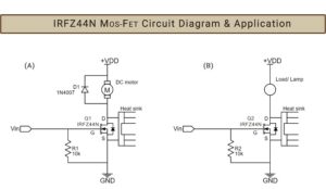
IRFZ44N Switch Circuit diagram for Arduino and General application:
Connecting an Arduino to the IRFZ44N is a simple process, which makes it adaptable for various applications, including IoT and as a relay driver for high-current loads like DC motors and DC Load. The following circuit illustrates how to connect a DC motor and load to the IRFZ44N MOSFET. Ensure proper pin connections to avoid short circuits, particularly for the drain and source.
Although not mandatory, but it’s recommended to include a Gate-Source resistor for circuit optimization. This versatility allowed due to the MOSFET’s ability to handle a wide range of input voltage and current, as indicated in the datasheet for this transistor. (refer the datasheet of this transistor).
For design purposes, you can consider using R(IN) with values of 100 Ohms or 220 Ohms and R(GS) with values of 10K or 100K-Ohm.
In the circuit diagram presented above, option (C) represents the simplest configuration for utilizing the IRF3205 to control various types of loads. Option (A) incorporates a fly-back diode in parallel to prevent reverse polarity voltage spikes from the DC motor, which can occur due to its inductive nature of a DC motor.
For high current switching applications, the IRF3205 MOSFET stands as a most popular and formidable player. As we know that high-powered devices plays an important role in various applications, from power amplifiers to motor control, so understanding its features, characteristics and capabilities is essential. This power MOSFET is renowned for its robustness and efficiency, making it a preferred choice for applications requiring high switching speeds and power handling capabilities.
In this post you get insights of IRF3205 pinout, application,schematic circuit, features, equivalent, and other details about how and where to use this high current N-channel MOSFET.
IRF3205 is manufactured by International Rectifier (now a part of Infineon Technologies), also prefix in the part number indicates the same. Extremely low on-resistance per silicon area, combined with the fast switching speed and high grade device design that HEXFET power MOSFETs are well known. At required power dissipation levels of up to approximately 50 watts, the low thermal resistance and low package cost, TO-220 packages are universally preferred in all commercial and industrial applications.
Main Features:
Maximum Rated voltage across Drain & Source → Vdss= upto 55V
Maximum operating current → Id = upto 110 Amps
Gate voltage → VGS(th) = 2V to 4V
Resistance → R(DS)(on)= 8.0 mΩ
Primary function → High current high speed switching.
Parameter Insight: IRF3205 power MOSFET is made for high power handling capability. It can handle drain to source voltage of up to 55 volts also The Gate voltage can be from 2 to 4 volts, i.e. can be turned on and off using a very small voltage as low as 2V. Its maximum operating current of 110 amps is achieved due to very low drain to source voltage of it mili-Ohm. These are the absolute maximum ratings, but to be on the safe side the operation of this transistor could be 80% of maximum ratings.
Package
TO-220
Transistor
Component
N-Channel
MOSFET
Drain to Source Voltage
55v
Max.
Gate to Source Voltage
±20V
Max.
Continues Drain Current
110A
Max.
Voltage Required to Conduct
2V to 4V
Min. (threshold voltage)
Drain Source Resistance
8mΩ
On state
Pulsed Drain Current
390A
Max.
Power Dissipation
200W
Max.
Switching time
@ Vdd=28V, Id=62A, Vgs=10V
Rise time
101nS
Typ.
Turn-On delay
14nS
Typ.
Turn-Off delay
50nS
Typ.
Fall time
65nS
Typ.
Internal Inductance & Capacitance
-
Check Datasheet below
Operating temperature
-55 to +170
Degree Centigrade
For detail characteristic like Vgs vs Id, Vds vs Ids, check and refer to the IRF3205 Datasheet below.
Always use proper heat sink if this mosfet is connected with high current application above 2 Amps to ensure proper operation and increase the life of MOSFET. If design is with space constrains, then you must solder mosfet ground to PCB metal ground.
How to test IRF3205 MOSFET if it is good or faulty?
(test are more accurate when it is done by removing mosfet from the PCB)
Check Gate Source: If multimeter display a voltage drop (around 0.5 to 0.7 volts) indicating a forward-biased when the positive probe (red) is connected to the gate (G) of the transistor IRF3205 and the negative probe (black) is connected to the source (S) in Diode Test mode.
Check Drain Source: If multimeter display a very high resistance (“OL” on the multimeter means ‘out of range’, means ‘open circuit’).
If any of the above, or both results are absent (or say don’t follow) then the MOSFET is faulty. Otherwise, it is good.
For more details on how to test MOSFET click here! (link)
Alternatives, Equivalent & Replacement: It is very popular and widely available MOSFET in the market, but in case you don’t have availability then you can go with alternatives. The alternatives for IRF3205 are IRFZ44N, IRF1405, IRF1407, IRF3305, IRFB3077, IRFB4110, IRF540N, 2N7000, FDV301N. Check this p channel power mosfet IRF4905
Application: Switching applications for controlling loads in IoT devices, Boost and buck converters, Solar inverters, DC motor speed control, Relay driver, SMPS (switch mode power supply), power inverter, embedded system, automation applications.
Interface the Arduino with IRF3205 is quite simple, also it can be used anywhere for IoT applications or use as a relay drive for driving or controlling the high current load like DC motor, lamp. The below circuit showing how to connect a DC motor and a DC load to IRF 3205 MOSFET. Make sure you connect the pin of MOSFET according to the pin diagram shown above. Drain and source connection should be taken care of to avoid short circuit.
It is not requisite to connect R(GS) and R(IN). But it is recommended to use Gate-Source resistor for circuit optimization. This is because this MOSFET is very versatile and design to handle wide variety of input voltage and current (refer the datasheet of this transistor).
For design purpose, you could use R(IN) = 100 Ohm or 220 Ohm; R(GS)= 10K or 100K
The circuit (C) in above image is the simplest form you can use IRF3205 for driving any kind of the load. The circuit (A) has a fly back diode used in parallel as shown is for preventing the reverse polarity voltage pulse from the DC motor due to inductive in nature.
IRF3205 Inverter circuit:
The IRF3205 inverter circuit is commonly used as 12V DC DIY inverters to get 110/230V AC, especially in medium to high-power applications. Inverters are the circuits that convert direct current (DC) from the battery into alternating current (AC). They find widespread use in various applications, including uninterruptible power supplies (UPS), solar inverters, motor drives, and more.
Here’s the feature that make IRF3205 MOSFET is implemented in inverter circuits, high power switching, PWM control, fast switching speed up to (100nS), high efficiency heat-dissipation, simple driving circuit.
The above circuit is designed using the CD4047 IC. The CD4047 is a CMOS oscillator/divider IC that can be configured to generate a square wave output, which is then used to drive a pair of complementary transistors or MOSFETs to create an AC output of 120/230V. The CD4047 IC is configured in astable mode to produce a square wave oscillation of frequency 50/60 Hz. It generates two output signals, Q and ~Q, with a 50{42041a7992ac3be9e9e29c856254fb498d8c7935d7cf8512da6802e8688e734a} duty cycle. You can read more on working of n-channel mosfet here.
The TP5100 is one of the most widely used battery charging controller IC/ BMS. It is a simple and cost-effective IC that is designed for large current portable electronic devices. One of the main advantages of the TP5100 IC is its compact and simple external circuit, and requires only a few basic additional components to function.
It has several safety features to protect the battery and the charger from being damaged. It can be easily purchased from online retailers or electronics suppliers as a module.
You could implement an 18650 battery charger circuit using TP5100 in two ways, one directly with the TP5100 module available in the market and the other with the TP5100 charger IC. Both are discussed and explained in detail below:
TP5100 is dual mode charging management chip, means it can charge 18650 battery or any 3.7v battery in two ways, one with the dual as well as single cell charging mode with 8.4V/ 4.2 volts.
Main features of TP5100:
Dual 8.4v / 4.2v operation for Li- ion cells.
Programmable charge current from 100mA -2000mA.
Wide operating voltage, from 5V to 18V, with SET/ Mode selection.
Charge Indicator: Blue LED – battery full/ standby; Red LED – charging indicator.
Pin
Remark
1,4,5,16 - VIN
Input supply voltage
2,3 - LX
Power drain MOS-FET connection
6 - PWR_ON¯
Enable/Disable IC (Float)
7 - GND
Ground return
8 - VS
Positive feedback for output current detection
9 - BAT+
Battery positive
10 - VREG
Internal power supply
11 - TS
Temperature sense of battery (refer to datasheet)
12- RTRICK
Trickle pre-charge current set
13 - CS
Chip select input (Float)
14 - STANDBY¯
Charging indicator
15 - CHRG¯
Full charge indicator
Specification:
Switching frequency 400Khz, usable inductance 22uH/ 33uH and more.
Size: 25 * 17 * 5mm ultra-small size.
Input operating voltage: 5-18V DC power supply.
PWR_ON Power battery for switching control.
Absolute maximum voltage: 20V
Operating temperature range: -40 ° to 85 °
BAT Short-Circuit Duration: Continuous.
Chip temperature protection, over-current protection, under-voltage protection.
Battery temperature protection, reverse battery shutdown, short circuit protection.
Steady pre-charge current programmable to 10% -100% of charging current.
TP5100 Application:
Portable equipment, lithium battery various chargers, Smartphone, Audio Bluetooth players, Industrial commercial power supply maintenance.
Below is the simple TP5100 Charging module schematic diagram for single cell li-ion and dual cell. The main IC of the module is the TP5100 chip, which is from manufacturer ‘Top Power ASIC’. It has become quite popular for charging 3.7V li ion batteries as it has all the required battery protection feature like over-charge, short circuit, under voltage and over-temperature protection.
For single battery circuit it uses the 4.2V charging voltage by default, but for dual cells in tp5100 charging module needs to connect ‘SET’ on the module board for 8.4V operation.
Below is the simple circuit diagram for the Li-ion battery charger schematic according to the datasheet of TP5100 with temperature sense disabled.
The Red LED glows when the battery is charging or module is in standby mode, and the Blue LED glows when the battery is fully charged. These indicators are connected to pin number 14 and pin number 15 respectively.
So here’s the TP5100 1s connection for single 3.7V li-ion battery.
The TP5100 module 2s connection manual for dual 3.7V li-ion batteries in series and 8.4 V is selected with ‘SET’ (short circuit).
Components required:
IC TP5100, 2x LED indicator, 3x Cap= 10.1uF (0.1uF || 10uF), 1x Cap= 0.1uF, Ind=22uH or 33uH, 1x Resistor= 1KΩ, Rs= 0.05Ω (2 x R100 SMD resistor 0.1Ω || 0.1Ω), 3.7V Lithium cells, micro USB/ USB C female connector, customized PCB.
Description:
This circuit can be used only for rechargeable battery charging purposes. Here, Rs is chosen to be 0.05Ω for 2000mA of output current. If we talk about TP 5100, it is a switching dc-dc buck regulator. Thus, in Mode 1 (1S), it is required to supply ~5V, and in Mode 2 (2S), it should be ~12V for intended operations.
Mode 1 (Default): You need to just connect 1 Lithium battery across BAT+, BAT- (GND); that’s all, the module will take care of charging process.
Mode 2 (SET): You need to connect 2 Lithium battery in series across BAT+, BAT- (GND); and Connect CS/ Pin 13 with VREG Pin 10 (for module pin “SET” to be connected) for correct charging process.
The charging current (IBAT) of the li-ion cell can be set manually by choosing the value of Rs. In all the modes during charging, the charging current could be determined as follows. The Rs(Ω) vs Ibat(mA) can be determined using the following table :
Note: If you have two 18650 lithium batteries, then by connecting them in series (short-circuit “SET” connections), each battery will charge at 1000mA of current. If you connect one Li-ion battery then it will charge it at the rate up to 2000mA, thus it will charge faster compared to TP4056 module to fully charge a battery.
There are several Charge Controller ICs available in the market, but here discussed popular ones are TP5100, and TP4056. It will help you choose the right one for your application.
TP5100 is an upgraded version of TP5000 with a maximum charging current of 2A. TP4056 is another charge controller IC with a maximum charging current of 1A.
IC TP5100
IC TP4056
Max. charging current
2000mA
1000mA
Li-ion cell
1s, 2s (single & dual cells)
1s (single cell)
Operating voltage/ Input
5V to 18V
5V to 8V
Charge voltage
4.2V, 8.4V
4.2V
Charging voltage control accuracy
>1%
~1.5%
Initial current
no soft-start
soft-start limits inrush current
In conclusion, TP5100 is a more advanced and flexible charge controller IC than TP4056. However, if you are looking for a simple and low-cost charge controller IC, TP4056 may be the right choice for you. The TP5100 is a good option for charging dual-cell lithium-ion or lithium-polymer batteries in power efficient applications.
Before choosing a charge controller IC, it is important to consider the requirements of your application, such as the charging current and charging time.
FAQ:
How many batteries can charge in TP5100?
You can charge one, two or more lithium battery cells with TP5100, but note that it has a max 2000mA of charging current. So, when charging multiple cells, you have to connect them in parallel. Also, the charging current will be divided among them, which will make charging slower. It is recommended to utilize two to four cells at a time with this module.
What is the output current of TP5100?
The maximum output current of TP5100 is 2000mA. It can be programmed to provide charging current from 100mA to 2000mA by changing the value of Rs.
What is the use of TP5100 module?
The TP5100 Module is used to charge either single or double 3.7 lithium-ion cell/ battery at 2Amp of current.
What is the input voltage of TP5100?
The input voltage of TP5100 is minimum 5V for single cell and 12- 18V for dual 3.7 lithium-ion cell.
When using a Leviton 4 way switch wiring diagram and setup, you can control the single light fixture from 3 different locations, while two locations can be operated by using a 3 way switch wiring diagram and setup. In this post you’re going to learn the wiring process for Leviton 4-way switch and 3 way switch setup in the traditional toggle switch configuration or with the modular/ decora. However, the wiring could be a little bit complex but very implementable by keeping proper terminology in consider. Let’s break down the process step by step for clarity.
Assumptions:
You have a single light fixture (bulb) that you want to control from three locations using traditional toggle switches.
You’re using standard electrical wiring, where Black wires are live/hot, White wires are neutral, and bare or green wires are ground.
Materials you’ll need:
Three 3-way toggle switches (labeled A, B)
One 4-way toggle switch (middle)
Electrical connecting wires (black, white, and green)
Wire nuts or other suitable connectors, screwdrivers, wire stripper/cutter.
Leviton 4 way switch wiring diagram:
In the below wiring diagram, one 4-way switch and two 3-way switch is used to control a load (LED bulb) from 3 different location) wiring diagram for older traditional toggle switches.
Leviton 4 Way Switch wiring diagram:
• Begin by attaching one terminal of the Light Bulb to the Common (here marked as “④”) terminal of the 3-way switch labeled ‘A’.
The other terminal of the Bulb should be connected to the Neutral wire (usually White) from the main power supply.• Now, proceed to link the Brass traveler wire labeled “②” from 3-way switch ‘A’ to the Output/Brass terminal of the 4-way switch (middle one).
Similarly, connect the Brass traveler wire “②” from 3-way switch ‘B’ to the Input/Black terminal of the 4-way switch.
• Finally, make a connection between the Black terminal labeled “①” of 3-way switch ‘B’ and the Line Hot/Live wire (typically Black) of the main power supply.
Connection with Leviton 3 way switch wiring diagram is way simpler than that of 4 way switch as we need to wire only two switches, discussed below in detail.
Assumptions:
• You have a single light fixture(LED bulb) that you want to control from 2 different locations using traditional toggle switches.
• You’re using standard electrical wiring, where Black wires are live/hot, White wires are neutral, and bare or green wires are ground.
Materials you’ll need:
• Two 3-way toggle switches.
• Electrical wires (black, white, and green)
• Wire nuts or other suitable connectors, screwdrivers, wire stripper/cutter.
3 way switch wiring Leviton:
• First, connect any one terminal of Load/ bulb to the Common (Black Screw) of the switch ‘B’. Then connect the 2nd terminal of Load to the Neutral/ (White wire) of the mains supply.
• Now, connect Common (Black screw) from switch ‘A’ to the Line Hot of the mains supply.
• Remaining are the Travelers connections, connect both the Travelers from switch ‘A’ to switch ‘B’. (Brass screw from switch ‘A’ to Brass screw of switch ‘B’)
• Don’t forget to connect the ground screws to the ground cable, commonly colored green.
Download 4 way switch wiring diagram PDF and 3 way switch wiring diagram PDF below.
Note: Leviton here is the trademark of the respective company, this website doesn’t own or claim any kind of copyright regarding the design of the switch.
Wiring a 4-way switch could be more complex as compared to a standard single-pole switch or a 3-way switch. It requires specific wiring connections and involves additional electrical connections other than live and neutral in the circuit. It is recommended to refer to the 4 way switch wiring diagrams when installing or wiring a 4-way switch to ensure safety and avoid short circuit over the wrong connections.
What is 4 way switches? Why it is used?
A 4-way switch is a type of electrical switch that is commonly used in residential and commercial buildings to control the lighting in a circuit from multiple locations. The 4 way switch wiring provides the means to turn on and off a light fixture independently, from up to four different switch locations. A long stare case or a large lobby can be an example for this kind of arrangement.
Here is the basic application diagram for simple understanding. This diagram showing the area of application of single pole switch, 3 way switch and a 4 way switch. Also remember some of the basic concepts along with the nomenclature and symbol for easy error free wiring. The different color is assigned to the screw for identifying the Common, Line and Ground.
Also, note that wiring can be different for switches from different manufacturer company, so always check notation/ nomenclature discussed below. There are different variants available that have same functionality but with different position of input-output connection screws, or we can say different arrangements. And this can be tricky sometime for the electrician to connect or troubleshoot, that what we have covered below, so keep reading.
A 4 way switch can not be used as a standalone, it is used in combination with some 3-way switches.
In a typical setup, you have two 3-way switches at either end of the circuit, and one or more 4-way switches in the middle. The 4-way switch acts as a connector between the 3-way switches, allowing the circuit to be controlled from multiple points.
How to wire a 4 way switch?
Below is the most commonly used modular type, (one way to wire a 4-way switch, two 3-way switch and one 4-way switch is used to control a load (LED bulb) from 3 different location) wiring diagram for modular and decora switches. (Output/ traveler pins on vertical axis)
Wiring a 4 Way Switch in 3 Simple Steps:
From two terminal of the (Bulb) Load, one terminal is connected to the Common /Black terminal of the 3 way switch ‘A’ , while the other end is connected to Neutral (White wire) to the mains supply. (120V AC, 60Hz)
Traveler terminal from ‘A’ are connected to the Output/ Brass terminal of a 4-Way switch.
Traveler terminal from ‘B’ are connected to Input/ Black terminal of a 4-Way switch.
Common/ Black terminal from ‘B’ is connected to the Line Hot/ Live (Black wire) to the supply.
The above steps to be applicable for all types of 4 way control wiring and all types of switch if you know how to identify the Line/ Live, Neutral, Common, Traveler terminals. That too are generally mentioned on the switch or in the technical documents comes along with the switches.
Below is the another way to wire a 4-way switch having Output or Traveler pins on diagonal axis. Two 3-way switches and one 4-way switch is required to implement the circuit (LED bulb) from 3 different location)
Important tips and tricks to remember while wiring:
(T) Travelers are INPUT’s/ OUTPUT’s for whatever reason in case of a 4-way switch, this is to be cleared up for your strange brain.
Don’t forget to connect the Green screw to the Ground/ Earth of the supply line.
There are no standards for the colors of wires on 3-way and 4-way switch travelers. The colors could vary depending on whether it is an NM cable or conduit.
With NM cable, the wire colors for travelers will be black and red using 3-wire cable. With conduit, the wire colors for travelers could be any color.
For your reminder, every switch vendor sometimes have their own way of arranging the terminals, so the switches shown here may not match what you have bought are. Therefore, it is recommended to observe and locate the terminal accordingly.
Below (in this wiring diagram, one 4-way switch and two 3-way toggle switch is used to control a load (LED bulb) from 3 different location) wiring diagram for older traditional toggle switches.
Wiring a 4 Way Traditional Switch Toggle type :
Step one is to connect one of the terminal from Bulb to the ④/ Common of 3-way switch ‘A’, and another terminal to Neutral (White wire) of the mains supply.
Now connect ②/ Brass traveler from 3-way switch ‘A’ to the Output/ Brass of the 4-way switch. Similarly, connect ②/ Brass traveler from 3-way switch ‘B’ to the Input/ Black of the 4-way switch.
At the end, connect the ①/ Black terminal from 3-way switch ‘B’ to the Line Hot/ Live (Black wire) of the mains supply.
(link to download page, file at the bottom of the page)
Safety Precautions:
To avoid fire, or fatal shock; turn off power at a circuit breaker or fuse and must ‘Ensure’ that power is off before wiring!
Installed or used in accordance with local electrical codes and regulations.
To clean, use a damp cloth without any soap or detergent. Do NOT use disinfecting products, including sprays or other types of atomized cleaning agents.
For those with a passion for technology and having an interest in the detail workings of modern connectivity, understanding the USB-C pinout is like uncovering the blueprint behind this remarkable connector. In this article, we will explore the vast and interesting detail of USB-C, which is serving to the modern electronics and to the tech enthusiasts, hobbyists, and engineers. Unraveling the complexities in simple words, and exploring the boundless possibilities it enables.
The USB C connector nowadays is most commonly used for charging mobile phones and various other portable devices like Bluetooth headset, Bluetooth speaker, Mini drones, Power Banks and various other tech gadgets not limited to emergency lights, LED decorative lamps.
To the left in the above image are USB connectors with board as a USB 2.0 mode utilization, (D+, D-, VBUS, GND). Note that the USB 3.0 are fully functional cables connections are implemented with 8 or 10 connecting wires/bus.
The 24-pin double-sided connector offers a USB-C port that measures 8.4 x 2.6 x 6.65 mm. The 8.4 millimeters (~0.33 inches) is its width, the 2.6 millimeters (~0.10 inches) is its height, and the depth of 6.65 millimeters (~0.262 inches). The dimensions are for the internal side of a receptacle and outer side of a plug. And for more details refer to the datasheet provided by the manufacturer.
These connectors come in two forms: a male/ plug and a female/ receptacle. (see image above)
The Plugs are commonly found on cables and adapters, providing the means to connect devices. On the other hand, receptacles can be found on devices and adapters, providing a socket for the plug to be inserted into and for establishing connections.
Simplified USB C pinout with their functions are as follows:
The USB C pinout table, offering resources on the intricate details of USB-C connectors. By reading the table, you could understand various pins and their vital functions, enabling a comprehensive understanding of how USB-C devices and cables work together in conjunction.
With careful attention to detail, the table unveils an array of essential pins such as VBUS, GND, CC1, CC2, D+, D- and so on. Each pin have a distinct purpose, from power supply and communication channels to data transmission and more.
It’s a complex network of connectivity enclosing power delivery, audio, video, and alternate modes. As you explore USB protocols, you’ll gain a profound insight of the complex signals and connections within the USB-C ecosystem.
Pin
Name
Description
Pin
Name
A1
GND
DC ground (+0V)
B12
GND
A2
TX1+
Super speed data transmit+ (host to device)
B11
TX2+
A3
TX1-
Super speed data transmit- (device to host)
B10
TX2-
A4
VDD
DC power (+5V)
B9
VDD
A5
CC1
Power delivery communication line
B8
CC2
A6
D+
Data transmit (host to device)
B7
D+
A7
D-
Data transmit (device to host)
B6
D-
A8
SBU1
Secondary bus
B5
SBU2
A9
VDD
DC power (+5V)
B4
VDD
A10
RX2-
Super speed data receive- (device to host)
B3
RX1-
A11
RX2+
Super speed data receive+ (host to device)
B2
RX1+
A12
GND
DC ground (+0V)
B1
GND
Below is an image showing USB type C 3.0 modules for high speed data communication:
Power: The A4, B4 and A9, B9 are connected to supply voltage. Also A1, B1 and A12, B12 are grounded. Thus, number of pins and wires to GND and VCC are reduced to 2 only.
SBU1, SUB2: These pins are called secondary bus. The A8, B8 are for side-band and are not utilized in USB communication and are reserved for future use. And therefore, the functional pins on each side remains to 9 each.
CC1 or CC2: These pins are used for Pin configuration detection, CC is used for USB-PD, i.e. USB power delivery communication to determine current control to the devices, for example charging current. Generally, CC is connected in series with a Resistor = 56k at port end. Thus, the total wires in the cable is found to be minimum 8 in numbers for functional high-speed USB C 3.0/ 3.1 type.
These cable supports both power and data transfer, there are also power only charging cables that support only charging. Meaning, you cannot use them for tasks such as syncing devices, transferring files, or connecting peripherals. They are solely intended for charging purposes. They come with only two connecting wires inside, and they are thicker wires to offer lower resistance to the current flowing though them.
These are made to target devices like neckband/ earphone charging, for charging mobile-phones, USB powered LED lamps and other gadgets that have nothing to do with the data transfer. They are less expensive than the one with data sync capability.
In this world of Electronics, a simple blinking LED circuit is a very basic yet very useful circuit. Blinking LEDs are often used in a wide range of Electronics projects from simple toys to gadgets, generally their blinking and flashing are programmed on a micro-controller or some kind of timer IC’s.
The LED flasher can be used to create a visual state indication, provide a warning signal or simply to add some stylishness to a project. The best thing is that creating a simple blinking LED circuit is relatively easy, even for those who are new to electronics and DIY.
In this article we will be discussing the basics of LED flasher circuit diagrams, including all the required components, the circuit schematic and programming if any. We will also provide step by step instruction on how to create your own Blinking LED circuit along with a few useful tips and tricks to help you get the most out of your project. Whether you are an occasional electronics enthusiast or just starting in this field, this article will provide you all the information you need to create your own LED flasher circuit and take your projects to the next level.
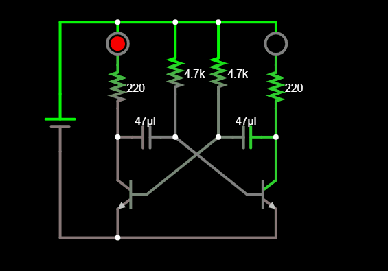
Blinking LED circuit with 555 Timer and only 5 components
The above image shows two red and blue indicators in and as a 555 timer blinking led circuit. This is a very simple blinking LED circuit consisting of only 5 components (except LEDs and battery). Strobe effect can be replicated with this circuit as it alternates red/blue color kinda cool though.
Its simplified connection is shown in the circuit diagram in two illustrations. You can solder it on a small compact PCB and make it portable/ versatile. Always check the polarity of the light emitting diode if anode and cathode are connected properly (incorrect polarity of LEDs is one of the most common errors).
The above circuit design implemented the design of the blinking LED with the help of timer IC 555. Out of three operation modes viz, astable mode, monostable mode, bistable mode. Here we have used the 555 timer IC in an Astable configuration.
Astable mode of operation gives two digital levels at the output, that is the output voltage will swing from high and low and low to high at regular intervals determined by RC network. This character of the astable output is used as a clock or square wave generator in various electrical circuits.
The Blinking LED circuit uses a pin number ‘3’ of 555 timer IC in astable mode, and will turn LED ON and OFF.
The duration of ON/ OFF is the duty cycle of the output square wave generated which can be changed by changing the value of the tank circuit. Also IC555 works with a wide range of voltage supply from 5V to 18V up to 200mA of load current.
All the All the circuit below uses a general purpose transistor so you can use any general purpose transistor available in your electronics project kits, you can use general transistors like BC 547 or 2N3904, BC 557, 2N2222, 2N2907 BC548,BC547. Please note that you can not substitute an NPN transistor with a PNP.
Simple One Transistor 2N3904/ BC547 LED flasher circuit
This circuit only uses the transistor’s Collector-Emitter terminal, keeping the Base terminal open. That circuit looks to be technically incorrect, however the above circuit diagram shows that even with just one transistor as the main component, you can create a working single LED flasher circuit. The circuit utilizes the negative resistance area in transistors to produce the blinking effect.
It is possible to change the flashing rate by changing either R11 or C4 or both together, but supply voltage must not be less than 9V otherwise the circuit does not work.
Even when the resistor R10 is short circuit it will work fine. The transistor in the 12V BC547 LED flasher circuit can be replaced with any general purpose NPN transistor.
Low Voltage Simple 1.5V/ 3V Single LED Flasher circuit
This circuit is very efficient and works only on as low as 1.5volts of supply, as this consumes current in the range of mAmps it lasts for very long without need to change the battery. You can power this circuit even with 3 volts and it would work fine.
3.7V/ 5V Blinking LED circuit using transistor
This is the tested and 100% working circuit of 3v LED flasher circuit, it utilizes a cross coupled transistor switching circuit as an astable multi-vibrator, but with lesser components than that of above which works on lower voltages like 3 volts and 5 volts.
The circuit shown above is the same as an Astable multivibrator design which is previously discussed above, using two transistors but with lesser components.
Blinking LED circuit using transistor in Astable Multivibrator mode
This circuit is made possible using the regenerative switching circuit. The circuit shown below is called an Astable Multivibrator design using two transistors. Astable Multi-vibrator are the most commonly used type of relaxation oscillator due to not only they are simple, reliable but also very simple to build. Also produces a constant square wave output signal which is used here in a bc547 led flasher circuit.
The video below is for reference only, flasher circuit is modified for only two resistors, it is recommended to connect all the required components if you are using this for high school projects.
The Astable Multivibrator is another type of cross-coupled transistor switching circuit that doesn’t have any stable output states, meaning its output changes from digital one to zero and vice versa. This circuit consists of two switching transistors, a cross-coupled feedback network, and two time delay capacitors which creates oscillation without the need of any external triggering circuit to produce square signals.
Here’s in short what happens in this circuit: The Capacitors C5 and C6 charge and discharge alternately through the resistors, that turns transistors off and on (cutoff region and saturation region). And thus the square waveform is created which in turns creates a flickering effect in LEDs. This can be better understand by using the below illustrations:
One can change the flickering speed of LED by changing the value of RC by using the below given formula as:
The Frequency of oscillation= Frequency of blinking= f
In the diagram below we have used D12 as an output control pin.1
The LEDs have one long leg (say, anode or positive leg). GND should be connected to the shorter leg of the LED (the negative leg, called the cathode) with the resistor 330Ω in series. And provide a power supply of 5V or whatever is available to you.
After you have built the circuit, open the Arduino Software (IDE). Connect the Arduino board to your computer and enter the following code into the IDE and dump the code to it.
Code for Blinking LED circuit:
const int LED_OUTPUT_PIN = 15;
void setup()
{
// set Pin 3 to output
pinMode(LED_OUTPUT_PIN, OUTPUT);
}
void loop() {
digitalWrite(LED_OUTPUT_PIN, HIGH); // turn LED on (output 5V)
delay(1000); // wait one second
digitalWrite(LED_OUTPUT_PIN, LOW); // turn LED off (output 0V)
delay(1000); // wait another second
}
Or
void setup()
{
// set Pin 3 to output
pinMode(15, OUTPUT);
}
void loop() {
digitalWrite(LED_OUTPUT_PIN, HIGH); // turn LED on (output 5V)
delay(1000); // wait one second
digitalWrite(LED_OUTPUT_PIN, LOW); // turn LED off (output 0V)
delay(1000); // wait another second
}
Click here for more detail on flickering led circuit using Arduino nano.
Conclusion:
All of the above circuits are well tested for blinking LED circuits for their output as an LED indications in a blinking pattern. Try all these circuits as it requires minimal components and costs are too affordable. Due to their simple design and basic mechanics involved, it can be experimented by individuals of all skill levels.
The TC4056 is a linear li-ion battery charger IC that is generally used in devices to charge 18650 li-ion cells. This is a charge controller IC which is designed to be used with all 3.7v of lithium ion cells, including Li-Polymer, Li-ion, and LiFePO4 batteries. In this article we will be discussing the circuit diagram of the TC4056 Lithium Ion Battery Charger module, components on the module.
If you are looking for alternatives to TC4056A then, there are several li-ion battery charger ICs such as the TP4056, TP5100, and TP5000. These ICs have similar functions to that of the TC4056A, but they have slightly different specifications, features and application.
The TP4056, TP5100, and TP5000 are alternatives to the TC4056, and they can be used as a substitute charge controller. Before selecting an alternative IC, it is essential to carefully examine the specific requirements of the application.
TC4056 Schematic & Circuit diagram
Below is the simple circuit diagram for the 3.7 V battery charger schematic according to the datasheet of TC4056 with temperature sense disabled. The circuit diagram for the TC4056A is simple, consisting of the main IC and a few supporting components such as resistors, capacitors, and LEDs. The schematic includes the input and output connections, as well as the output current control.
In the charging phase, only the Red LED glows, and in the fully charged state, only the Green LED glows. These indicators are connected to pin number 7 and pin number 6 respectively.
So here’s the diagram: How to wire a TC4056?
Components required:
IC TC4056, 2x LED indicator, 2x Cap= 10uF, Rprog= 1.2KΩ, 2x Resistor= 1KΩ, Rs= 0.4Ω, 3.7V Lithium cell, micro usb/ usb c female connector, pcb.
Note:
This circuit can be used only for charging purposes. Rprog is chosen to be 1.2KΩ for 1000mA of output current, this can be changed by setting different values of Rprog. If Rprog is chosen to be 2KΩ then battery will be charge at 580mA of output current.
You can manually set the charging current (IBAT) of the lithium ion cell by selecting a value for the Rprog value. In all modes during charging, the voltage on pin 2 can be calculated with respective to charging current as follows:
The Rprog(KΩ) vs Ibat(mA) can be determined using following table:
The TC4056A and its alternatives ICs have the battery protection features to ensure safe and reliable charging. Like, it has over-voltage protection, which prevents the battery from being charged to a voltage level that is too high. It also has thermal protection, which cuts off the current when the chip gets overheated due to any reason, and also has short-circuit protection.
TC4056 Module:
IC TC4056 is also available as a module, which has all the components on board required for functioning. This module makes it easy for DIY projects, as it eliminates the need for manual soldering and component placement. TC4056A modules can be purchased online or through electronic component distributors.
TC4056 Pinout:
The TC4056 has a total of eight pins, all of them are used in the schematics. The pinout of the TC4056A is as follows:
VCC+: This is the positive input terminal.
PROG-: This is the terminal for determining the charging current.
BAT+: This is the positive terminal of the battery being charged.
CHRG: This is the indicator pin of the battery being charged.
STDBY: This is the status output pin, which indicates the battery is not connected.
GND: This is the ground pin.
TEMP: This is the thermal protection pin, which provides protection against overheating.
CE: This is the charge enable pin, ie., switch for charging process.
The pinout of the TC4056A and its circuit diagram are also straightforward and well-documented, making it easy to use in a variety of battery charging applications.

")


")