IRF3205, Datasheet PDF, Specification, Circuits, Pinout, Equivalent, Alternatives
For high current switching applications, the IRF3205 MOSFET stands as a most popular and formidable player. As we know that high-powered devices plays an important role in various applications, from power amplifiers to motor control, so understanding its features, characteristics and capabilities is essential. This power MOSFET is renowned for its robustness and efficiency, making it a preferred choice for applications requiring high switching speeds and power handling capabilities.
In this post you get insights of IRF3205 pinout, application,schematic circuit, features, equivalent, and other details about how and where to use this high current N-channel MOSFET.
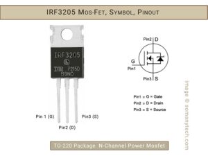
IRF3205 is manufactured by International Rectifier (now a part of Infineon Technologies), also prefix in the part number indicates the same. Extremely low on-resistance per silicon area, combined with the fast switching speed and high grade device design that HEXFET power MOSFETs are well known. At required power dissipation levels of up to approximately 50 watts, the low thermal resistance and low package cost, TO-220 packages are universally preferred in all commercial and industrial applications.
Main Features:
Maximum Rated voltage across Drain & Source → Vdss= upto 55V
Maximum operating current → Id = upto 110 Amps
Gate voltage → VGS(th) = 2V to 4V
Resistance → R(DS)(on)= 8.0 mΩ
Primary function → High current high speed switching.
Click here! for 9v to 5v converter circuit.
Parameter Insight:
IRF3205 power MOSFET is made for high power handling capability. It can handle drain to source voltage of up to 55 volts also The Gate voltage can be from 2 to 4 volts, i.e. can be turned on and off using a very small voltage as low as 2V. Its maximum operating current of 110 amps is achieved due to very low drain to source voltage of it mili-Ohm. These are the absolute maximum ratings, but to be on the safe side the operation of this transistor could be 80% of maximum ratings.
| Package | TO-220 | Transistor |
|---|---|---|
| Component | N-Channel | MOSFET |
| Drain to Source Voltage | 55v | Max. |
| Gate to Source Voltage | ±20V | Max. |
| Continues Drain Current | 110A | Max. |
| Voltage Required to Conduct | 2V to 4V | Min. (threshold voltage) |
| Drain Source Resistance | 8mΩ | On state |
| Pulsed Drain Current | 390A | Max. |
| Power Dissipation | 200W | Max. |
| Switching time | @ Vdd=28V, Id=62A, Vgs=10V | |
| Rise time | 101nS | Typ. |
| Turn-On delay | 14nS | Typ. |
| Turn-Off delay | 50nS | Typ. |
| Fall time | 65nS | Typ. |
| Internal Inductance & Capacitance | - | Check Datasheet below |
| Operating temperature | -55 to +170 | Degree Centigrade |
For detail characteristic like Vgs vs Id, Vds vs Ids, check and refer to the IRF3205 Datasheet below.
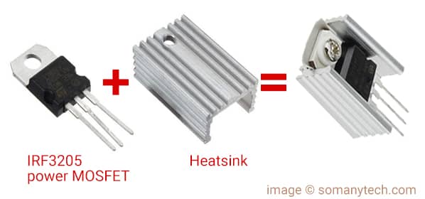
Always use proper heat sink if this mosfet is connected with high current application above 2 Amps to ensure proper operation and increase the life of MOSFET. If design is with space constrains, then you must solder mosfet ground to PCB metal ground.
How to test IRF3205 MOSFET if it is good or faulty?
(test are more accurate when it is done by removing mosfet from the PCB)
- Check Gate Source: If multimeter display a voltage drop (around 0.5 to 0.7 volts) indicating a forward-biased when the positive probe (red) is connected to the gate (G) of the transistor IRF3205 and the negative probe (black) is connected to the source (S) in Diode Test mode.
- Check Drain Source: If multimeter display a very high resistance (“OL” on the multimeter means ‘out of range’, means ‘open circuit’).
If any of the above, or both results are absent (or say don’t follow) then the MOSFET is faulty. Otherwise, it is good.
For more details on how to test MOSFET click here! (link)
Alternatives, Equivalent & Replacement:
It is very popular and widely available MOSFET in the market, but in case you don’t have availability then you can go with alternatives. The alternatives for IRF3205 are IRFZ44N, IRF1405, IRF1407, IRF3305, IRFB3077, IRFB4110, IRF540N, 2N7000, FDV301N. Check this p channel power mosfet IRF4905
Application:
Switching applications for controlling loads in IoT devices, Boost and buck converters, Solar inverters, DC motor speed control, Relay driver, SMPS (switch mode power supply), power inverter, embedded system, automation applications.
IRF3205 Datasheet PDF:
Download IRF3205 datasheet PDF here. (link)
IRF3205 Switch Circuit diagram:
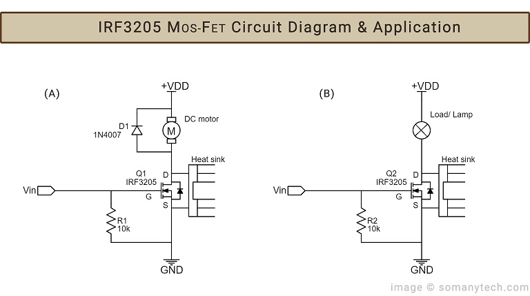
Interface the Arduino with IRF3205 is quite simple, also it can be used anywhere for IoT applications or use as a relay drive for driving or controlling the high current load like DC motor, lamp. The below circuit showing how to connect a DC motor and a DC load to IRF 3205 MOSFET. Make sure you connect the pin of MOSFET according to the pin diagram shown above. Drain and source connection should be taken care of to avoid short circuit.
It is not requisite to connect R(GS) and R(IN). But it is recommended to use Gate-Source resistor for circuit optimization. This is because this MOSFET is very versatile and design to handle wide variety of input voltage and current (refer the datasheet of this transistor).
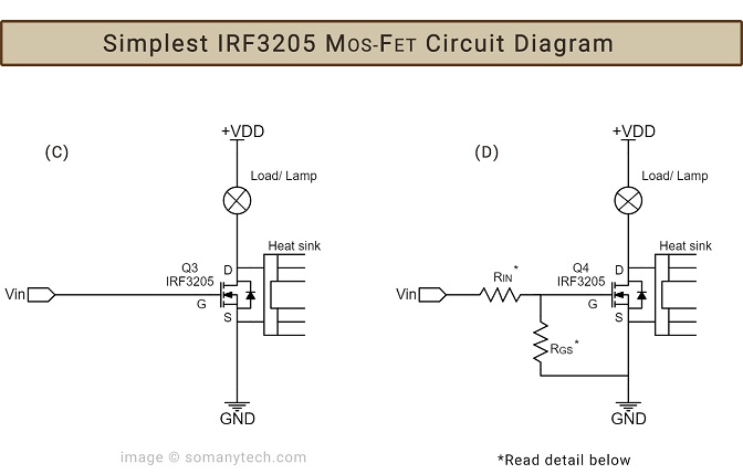
For design purpose, you could use R(IN) = 100 Ohm or 220 Ohm; R(GS)= 10K or 100K
The circuit (C) in above image is the simplest form you can use IRF3205 for driving any kind of the load. The circuit (A) has a fly back diode used in parallel as shown is for preventing the reverse polarity voltage pulse from the DC motor due to inductive in nature.
IRF3205 Inverter circuit:
The IRF3205 inverter circuit is commonly used as 12V DC DIY inverters to get 110/230V AC, especially in medium to high-power applications. Inverters are the circuits that convert direct current (DC) from the battery into alternating current (AC). They find widespread use in various applications, including uninterruptible power supplies (UPS), solar inverters, motor drives, and more.
Here’s the feature that make IRF3205 MOSFET is implemented in inverter circuits, high power switching, PWM control, fast switching speed up to (100nS), high efficiency heat-dissipation, simple driving circuit.
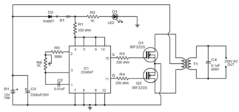
The above circuit is designed using the CD4047 IC. The CD4047 is a CMOS oscillator/divider IC that can be configured to generate a square wave output, which is then used to drive a pair of complementary transistors or MOSFETs to create an AC output of 120/230V. The CD4047 IC is configured in astable mode to produce a square wave oscillation of frequency 50/60 Hz. It generates two output signals, Q and ~Q, with a 50{42041a7992ac3be9e9e29c856254fb498d8c7935d7cf8512da6802e8688e734a} duty cycle. You can read more on working of n-channel mosfet here.


